Electronic devices and methods for making same using nanotube regions to assist in thermal heat-sinking

a technology of nanotubes and electrical components, applied in the field of electrical components, can solve the problems of thermal limitation, degraded devices, solder bumps limiting the thermal transport out of light emitting diodes,

Inactive Publication Date: 2005-01-13
GE LIGHTING SOLUTIONS LLC
View PDF6 Cites 155 Cited by
  • Summary
  • Abstract
  • Description
  • Claims
  • Application Information

AI Technical Summary

Problems solved by technology

To achieve improved light output, these devices are being driven with increasingly higher currents, resulting in thermally limited performance.
This involves substantial heating near the active layers which can degrade the device.
These thick solder bumps can limit thermal transport out of the light emitting diode die.

Method used


Image

  • Electronic devices and methods for making same using nanotube regions to assist in thermal heat-sinking
  • Electronic devices and methods for making same using nanotube regions to assist in thermal heat-sinking
  • Electronic devices and methods for making same using nanotube regions to assist in thermal heat-sinking

Examples


Embodiment Construction

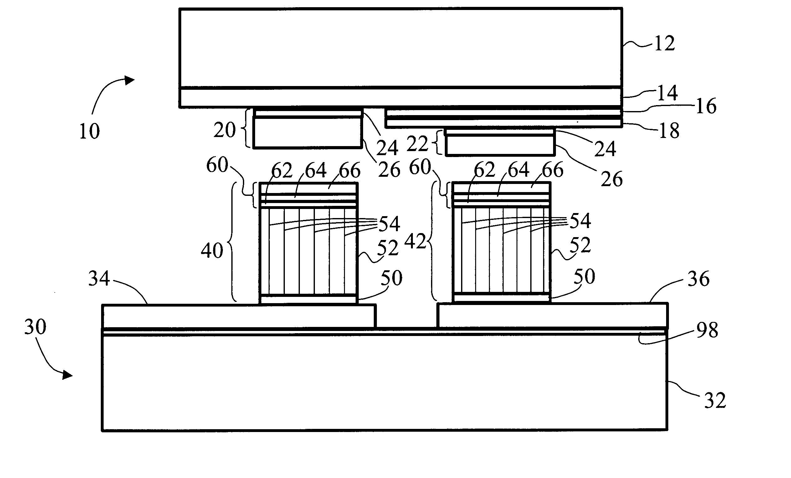
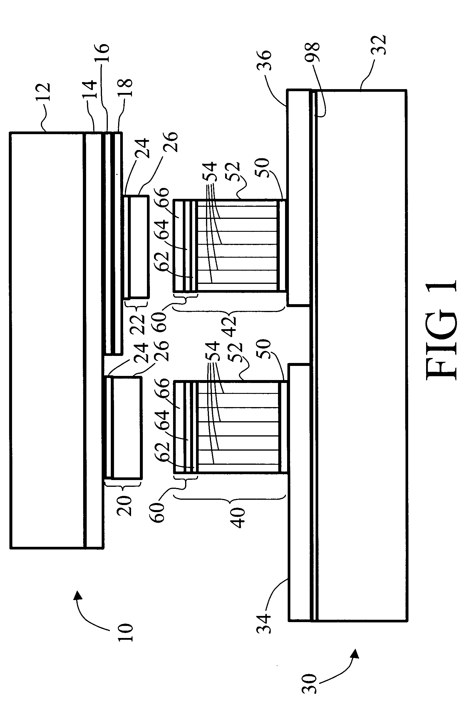
[0018] With reference to FIG. 1, a flip-chip light emitting diode die 10 is shown in position for die-bonding. The light emitting diode 10 includes a transparent substrate 12 and active layers 14, 16, 18 deposited on the substrate 12. In one suitable embodiment, the transparent substrate is sapphire or silicon carbide, and the active layers 14, 16, 18 are deposited by metal-organic chemical vapor deposition (also known by similar nomenclatures such as organometallic vapor phase epitaxy), molecular beam epitaxy, or another epitaxial film growth technique. The active layers 14, 16, 18 define a GaN-based p-on-n or n-on-p light emitting diode structure in which the layers 14, 18 are of opposite conductivity type and the interposed layer 16 defines an electron-hole pair recombination region at which electrons and holes from the outer layers 14, 18 recombine.

[0019] In some GaN-based light emitting diodes, the layer 16 is omitted and radiative recombination occurs principally around a jun...


PUM


Abstract

A semiconductor device die (10, 116) is disposed on a heat-sinking support structure (30, 100). Nanotube regions (52, 120) contain nanotubes (54, 126) are arranged on a surface of or in the heatsinking support structure (30, 100). The nanotube regions (52, 120) are arranged to contribute to heat transfer from the semiconductor device die (10, 116) to the heat-sinking support structure (30, 100). In one embodiment, the semiconductor device die (10) includes die electrodes (20, 22), and the support structure (30) includes contact pads (40, 42) defined by at least some of the nanotube regions (52). The contact pads (40, 42) electrically and mechanically contact the die electrodes (20, 22). In another embodiment, the heat-sinking support structure (100) includes microchannels (120) arranged laterally in the support structure (100). At least some of the nanotube regions are disposed inside the microchannels (100).

Description

BACKGROUND [0001] The present invention relates to the electronics arts. It especially relates to flip-chip bonded light emitting diodes for lighting applications, and will be described with particular reference thereto. However, the invention will also find application in conjunction with die-bonding and cooling of other electronic devices. [0002] Light emitting diodes are increasingly being employed in outdoor displays and signals, indoor illumination, and other applications that call for high levels of light output. To achieve improved light output, these devices are being driven with increasingly higher currents, resulting in thermally limited performance. [0003] To improve heat removal, flip-chip mounted light emitting diodes have been developed. In the flip-chip arrangement, the active light emitting layers are grown on a transparent substrate, front-side contacts are fabricated on the light emitting layers, and the die is bonded front-side down to a lead frame, heat sink, or ...

Claims


Application Information

Patent Timeline
Patent Type & Authority Applications(United States)
IPC IPC(8): F28F13/18H01L23/373H01L23/473H01L23/485H01L33/62H01L33/64
CPCB82Y10/00F28F13/185H01L24/13H01L2224/1703H01L2224/06102H01L2224/0401H01L2924/12041H01L2924/014H01L2924/01033H01L2924/01006H01L2924/00013H01L2924/19042H01L2924/01082H01L23/373H01L23/473H01L24/10H01L24/81H01L33/62H01L33/648H01L2224/1308H01L2224/13084H01L2224/13144H01L2224/13155H01L2224/13166H01L2224/81193H01L2224/81205H01L2224/81801H01L2224/81894H01L2924/01005H01L2924/01013H01L2924/01015H01L2924/01018H01L2924/01022H01L2924/01029H01L2924/01057H01L2924/01074H01L2924/01075H01L2924/01079H01L2924/00014H01L2224/13099H01L2924/00H01L2224/13H01L2924/12042
Inventor ARIK, MEHMETWEAVER, STANTON E. JR.CARNAHAN, JAMES C.BECKER, CHARLES A.GERSTLER, WILLIAM D.
Owner GE LIGHTING SOLUTIONS LLC
Why Eureka
Try Eureka