Pixel circuit, display device, and driving method of pixel circuit

a technology of pixel circuit and display device, which is applied in the direction of identification means, instruments, manufacturing tools, etc., can solve the problems of inability to correct the variation of mobility, the uniformity of image quality will deteriorate, and the difficulty of realizing a large sized and high definition display. achieve the effect of high quality imag

Inactive Publication Date: 2005-01-13
SONY CORP
View PDF6 Cites 301 Cited by
  • Summary
  • Abstract
  • Description
  • Claims
  • Application Information

AI Technical Summary

Benefits of technology

[0034] An object of the present invention is to provide a pixel circuit, a display device, and a driving method of the pixel circuit able to stably and correctly supply a current having a desired value to the light emi

Problems solved by technology

An organic EL display, in the same way as a liquid crystal display, may be driven by a simple matrix and an active matrix system, but while the former has a simple structure, it has the problem that realization of a large sized and high definition display is difficult.
As a result, the uniformity of the image quality will deteriorate.
In the pixel circuit of FIG. 3, however, even if the Vth variation can be corrected, the variation of the mobility μ cannot be corrected.
That is, a large current flows, the current value ends up being affected by the variation of the mobility

Method used


Image

  • Pixel circuit, display device, and driving method of pixel circuit
  • Pixel circuit, display device, and driving method of pixel circuit
  • Pixel circuit, display device, and driving method of pixel circuit

Examples


first embodiment

[0079] First Embodiment

[0080]FIG. 8 is a block diagram of the configuration of an organic EL display device employing pixel circuits according to the first embodiment. FIG. 9 is a circuit diagram of the concrete configuration of a pixel circuit according to the first embodiment in the organic EL display device of FIG. 8.

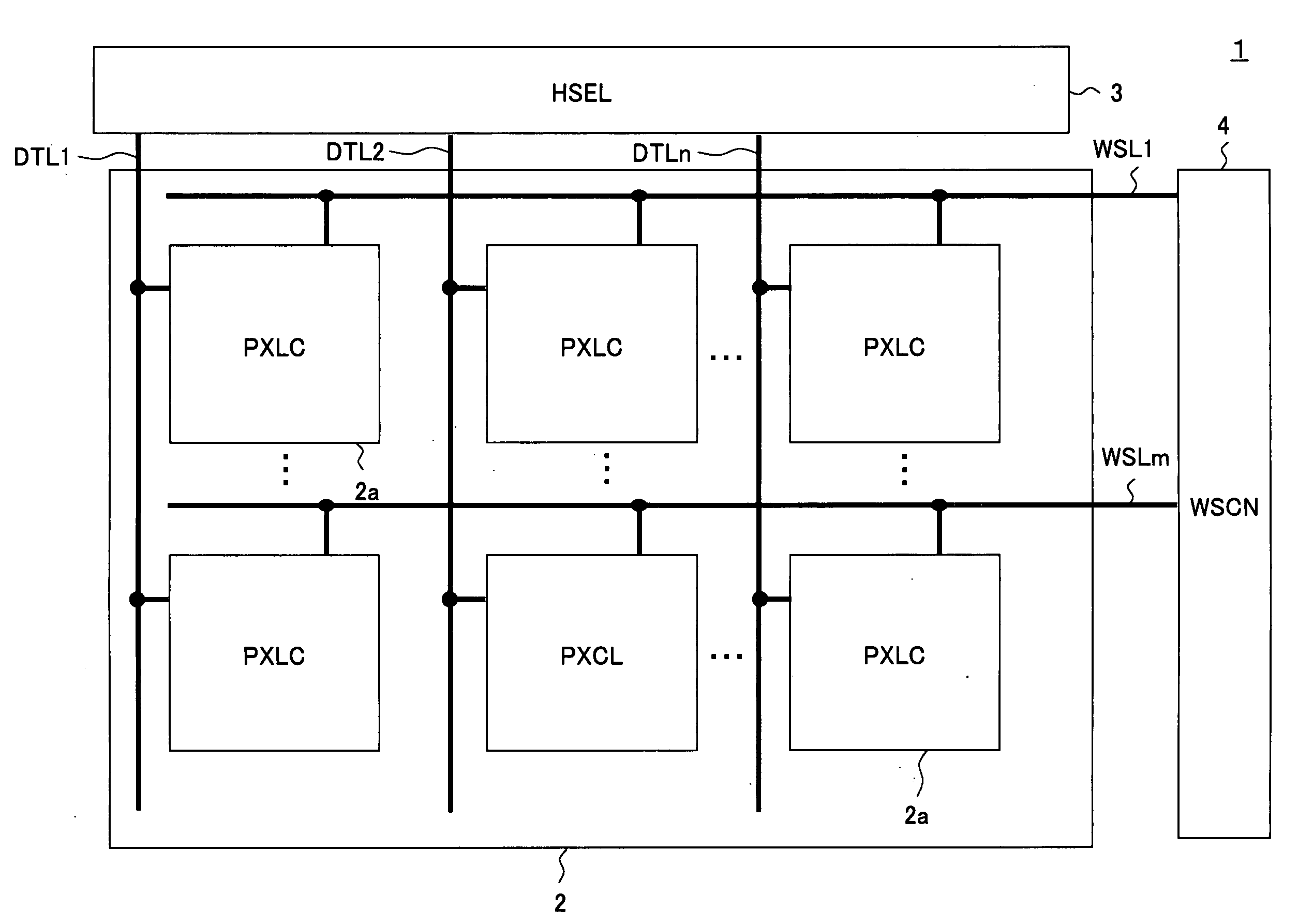
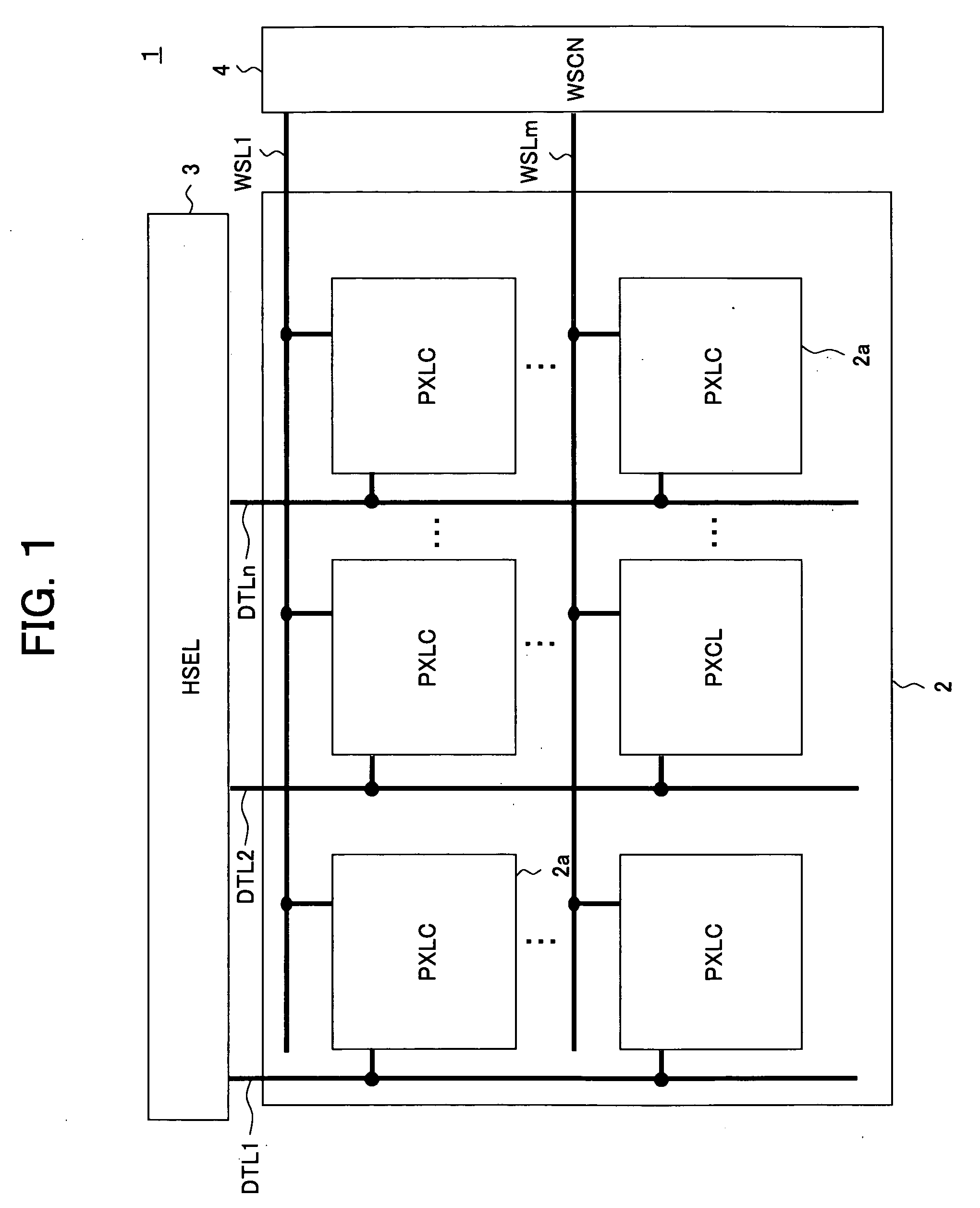
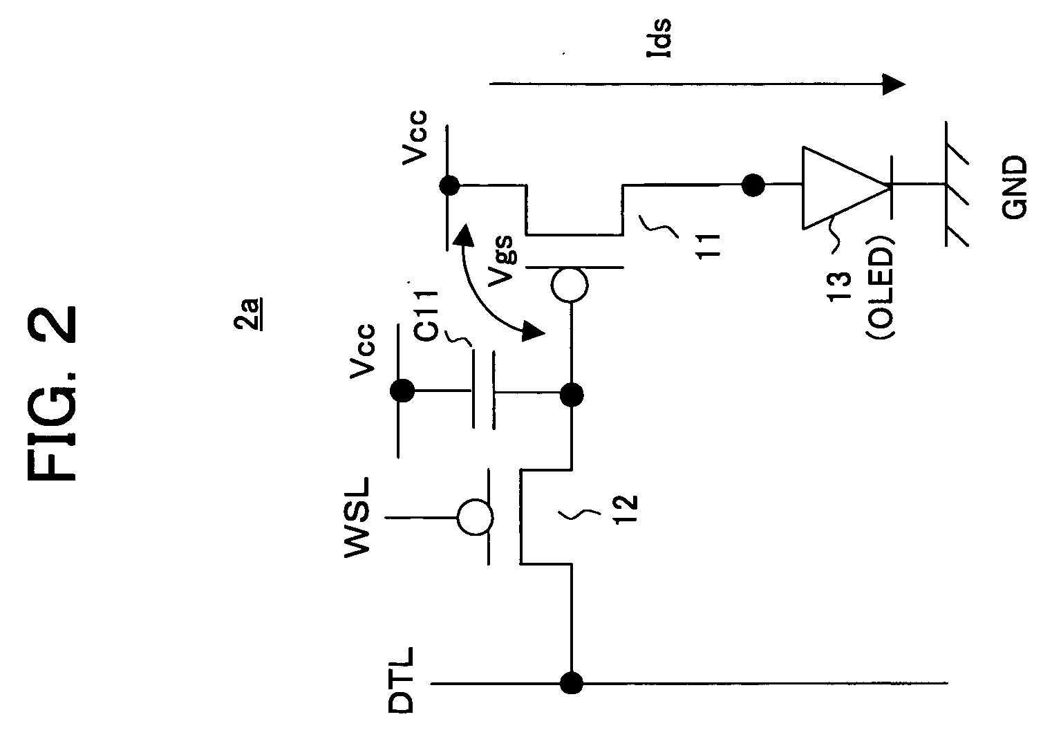
[0081] This display device 100 has, as shown in FIG. 8 and FIG. 9, a pixel array portion 102 having pixel circuits (PXLC) 101 arranged in an m×n matrix, a horizontal selector (HSEL) 103, a write scanner (WSCN) 104, a drive scanner (DSCN) 105, an auto-zero circuit (AZRD) 106, a reference constant current source (RCIS) 107, data lines DTL101 to DTL10n selected by the horizontal selector 103 and supplied with a data signal in accordance with the luminance information, scanning lines WSL101 to WSL10m selectively driven by the write scanner 104, drive lines DSL101 to DSL10m selectively driven by the drive scanner 105, auto-zero lines AZL101 to AZL10m selectively driven b...

second embodiment

[0099] Second Embodiment

[0100]FIG. 13 is a block diagram of the configuration of an organic EL display device employing pixel circuits according to a second embodiment. FIG. 14 is a circuit diagram of the concrete configuration of a pixel circuit according to the second embodiment in the organic EL display device of FIG. 13.

[0101] The difference of the second embodiment from the first embodiment mentioned above resides in that, instead of a configuration wherein a reference constant current source (RCIS) 107 is provided, the reference current is passed through the reference current supply line, and the first node ND111 and the reference current supply line are connected by the TFT 115 of each pixel circuit, as shown in FIG. 14, the configuration was made so that the reference current was generated for every pixel circuit. Concretely, as shown in FIG. 14, in each pixel circuit 101A, an n-channel TFT 117 serving as the constant current source, and a constant voltage source 118 are pr...

third embodiment

[0105] Third Embodiment

[0106]FIG. 15 is a block diagram of the configuration of an organic EL display device employing pixel circuits according to a third embodiment. FIG. 16 is a circuit diagram of the concrete configuration of a pixel circuit according to the third embodiment in the organic EL display device of FIG. 15.

[0107] The difference of the third embodiment from the above second embodiment resides in that the constant voltage source 108 is provided and in that common voltage supply lines VSL101 to VSL10n are laid for every column and connected to the gates of TFT 117 of the pixels. The voltage source V108 is connected to the voltage supply lines VSl101 to VSL10n.

[0108] The rest of the configuration is the same as the second embodiment.

[0109] According to the third embodiment, the same effects as those of the first embodiment mentioned above can be obtained.


PUM


Abstract

A pixel circuit able to stably and correctly supply a current having a desired value to a light emitting diode of each pixel without being influenced by variation of a threshold value of an active element inside the pixel or variation of mobility and able to display a high quality image as a result of this, wherein a TFT as a fourth switch is turned on together with a TFT as a second switch at the time of an auto-zero operation, a reference current line is connected to a drive transistor of the pixel through a first node, and the variation of the threshold value Vth is corrected, whereby variation of the on current due to the mobility at the time of a white display can be suppressed and the uniformity with respect to variation in the mobility can be greatly enhanced, and a display device and a driving method of the pixel circuit.

Description

BACKGROUND OF THE INVENTION [0001] 1. Field of the Invention [0002] The present invention relates to a pixel circuit having an organic electroluminescence (EL) element or other electro-optic element with a luminance controlled by a current value and an image display device comprised of such pixel circuits arrayed in a matrix, in particular a so-called active matrix type image display device controlled in value of current flowing through the electro-optic elements by insulating gate type field effect transistors provided inside the pixel circuits, and a driving method of the pixel circuits. [0003] 2. Description of the Related Art [0004] In an image display device, for example, a liquid crystal display, a large number of pixels are arranged in a matrix and the light intensity is controlled for every pixel in accordance with the image information to be displayed so as to display an image. This same is true for an organic EL display etc. An organic EL display is a so-called self light ...

Claims


Application Information

Patent Timeline
IPC IPC(8): H01L51/50G09F9/30G09G3/20G09G3/30G09G3/32G09G3/36G09G5/00H05B33/00H05B33/14
CPCG09G3/3233G09G2300/043G09G2300/0809G09G2300/0819G09G2320/043G09G2300/0852G09G2300/0861G09G2310/0262G09G2300/0842B25C1/005
Inventor YAMASHITA, JUNICHIUCHINO, KATSUHIDEYAMAMOTO, TETSURO
Owner SONY CORP
Why Eureka
Try Eureka