Automated wafer defect inspection system and a process of performing such inspection

a defect inspection and automatic technology, applied in semiconductor/solid-state device testing/measurement, image enhancement, instruments, etc., can solve the problems of high equipment and large equipment, expensive and large inspection devices are not cost justifiable for smaller shops, and none of these systems address the particular and unique constraints. , to achieve the effect of improving process control and improving inspection quality

Inactive Publication Date: 2005-01-13
RUDOLPH TECHNOLOGIES INC
View PDF99 Cites 84 Cited by
  • Summary
  • Abstract
  • Description
  • Claims
  • Application Information

AI Technical Summary

Benefits of technology

[0027] It is further an objective of the present invention to provide an automated defect inspection system that provides for improved inspection quality and consistency.
[0028] It is further an objective of the present invention to provide an automated defect inspection system that provides for improved process control.
[0029] It is further an objective of the present invention to provide an automated defect inspection system that has inspection recipes therein and can create, copy and edit such recipes to customize the system to the user's inspection requirements.

Problems solved by technology

Often this equipment is very expensive and large.
At the 1st inspection stage, this expense and machine size issue is not as significant as at later inspection stages because only a relatively few parties manufacture the silicon wafers and thus need to inspect bare wafers in comparison to the vast number of companies that buy bare or sawn wafers and further process them into finished chips.
These often expensive and large inspection devices are not cost justifiable for smaller shops and as such, inspection equipment is needed that satisfies this need at the 2nd and 3rd stages as well as is more economical for the vast many smaller companies that finish process wafers.
However, none of these systems address the particular and unique constraints of 2nd optical and this area has been largely ignored.
This manual process is inaccurate due to various factors including stress, eye fatigue and boredom of the operator as well as different perceptions by different operators as to the significance of a finding.
In addition, smaller circuit geometry and higher throughput requirements are increasing the demands on semiconductor inspection at this 2nd optical level, all of which further results in operator stress, eye fatigue, and sometimes lower quality.

Method used


Image

  • Automated wafer defect inspection system and a process of performing such inspection
  • Automated wafer defect inspection system and a process of performing such inspection
  • Automated wafer defect inspection system and a process of performing such inspection

Examples


Embodiment Construction

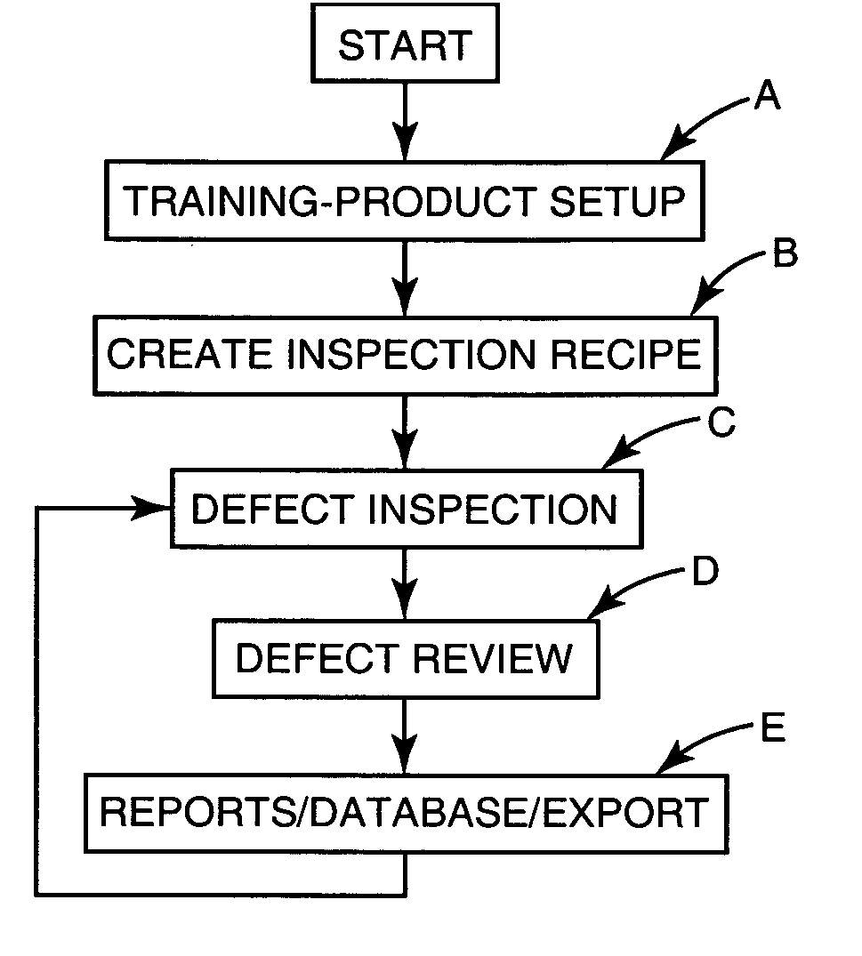
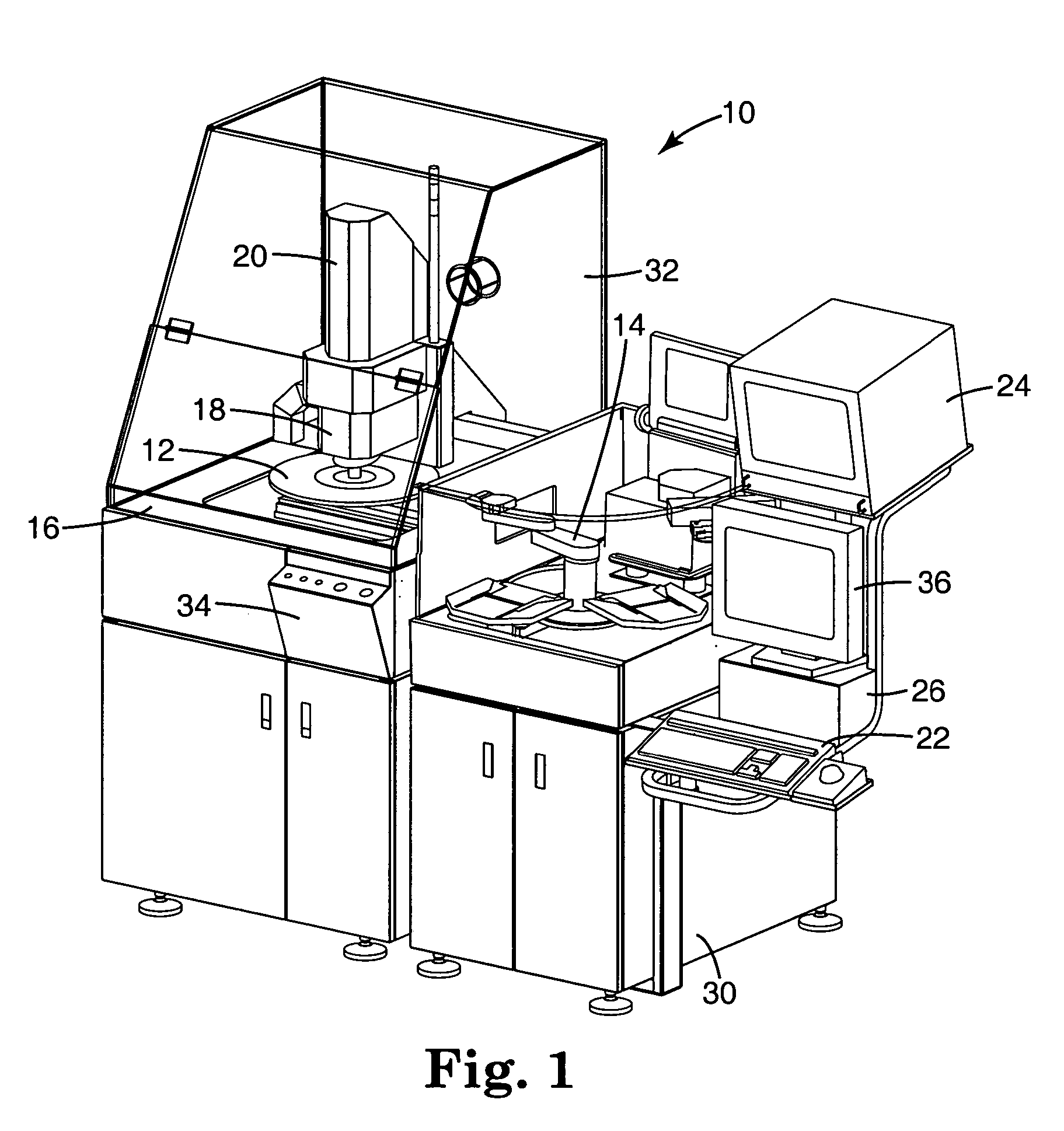
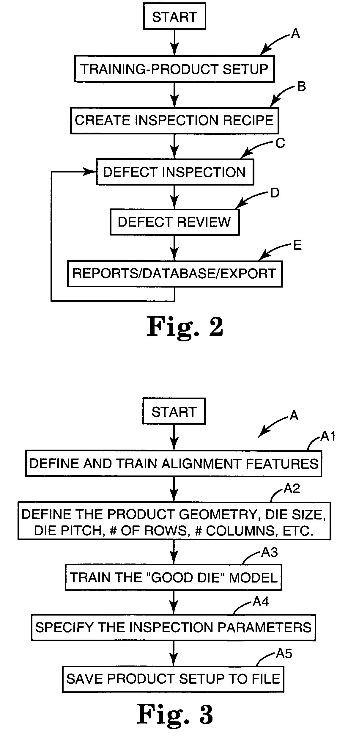
[0075] The automated defect inspection system of the present invention is indicated generally at 10 as is best shown overall in FIGS. 1 and 8 (but in detailed portions in FIGS. 2-7 and 9-21) and is used in one environment to find defects on die on patterned wafers W but is intended for this and other uses including for inspecting whole wafers, sawn wafers, broken wafers, wafers of any kind on film frames, die in gel paks, die in waffle paks, MCMs, JEDEC trays, Auer boats, and other wafer and die package configurations (although hereinafter all of these uses shall be referred to generally as inspection of wafers W). The system inspects for many types of defects including, but not limited to, the following: metalization defects (such as scratches, voids, corrosion, bridging, etc.), diffusion defects, passivation layer defects, scribing defects, glassivation defects, chips and cracks from sawing, probe or bond area defects (such as missing probe marks, discoloration, missing metal and ...


PUM

PropertyMeasurementUnit
angleaaaaaaaaaa
angleaaaaaaaaaa
angleaaaaaaaaaa

Abstract

An automated defect inspection system has been invented and is used on patterned wafers, whole wafers, broken wafers, partial wafers, sawn wafers such as on film frames, JEDEC trays, Auer boats, die in gel or waffle packs, MCMs, etc. and is specifically intended and designed for second optical wafer inspection for such defects as metalization defects (such as scratches, voids, corrosion, and bridging), diffusion defects, passivation layer defects, scribing defects, glassivation defects, chips and cracks from sawing, solder bump defects, and bond pad area defects.

Description

REFERENCE TO RELATED APPLICATION [0001] This application claims the benefit of U.S. Provisional Application Nos. 60 / 092923 and 60 / 092701, filed on Jul. 15, 1998, and U.S. patent application Ser. No. 09 / 352,564, filed on Jul. 13, 1999.BACKGROUND OF THE INVENTION [0002] 1. Technical Field [0003] The present invention relates to defect inspection systems for the semiconductor industry. More particularly, the present invention relates to an automated defect inspection system for patterned wafers, whole wafers, sawn wafers such as on film frames, JEDEC trays, Auer boats, die in gel or waffle packs, multi-chip modules often referred to as MCMs, etc. that is specifically intended and designed for second optical wafer inspection for such defects as metalization defects (such as scratches, voids, corrosion, and bridging), diffusion defects, passivation layer defects, scribing defects, glassivation defects, chips and cracks from sawing, and bump or bond pad area defects such as gold or solder...

Claims


Application Information

Patent Timeline
Patent Type & Authority Applications(United States)
IPC IPC(8): G01N21/956G06T1/00G01B11/30H01L21/00H01L21/66
CPCG01N21/9501H01L21/67242H01L21/67271H01L21/67288H01L2924/0002H01L22/12H01L2924/00H04N23/56G01N21/8803G01N21/8806G01N2021/8838G01N2201/06113G01N2201/0696G01N2201/0697G01N2201/12G06T7/0004G06T2207/30148
Inventor O'DELL, JEFFREYVERBURGT, THOMASHARLESS, MARKWATKINS, CORY
Owner RUDOLPH TECHNOLOGIES INC
Why Eureka
Try Eureka