Manufacturing method for semiconductor device

a manufacturing method and semiconductor technology, applied in semiconductor devices, semiconductor/solid-state device details, electrical devices, etc., can solve the problems of reducing the reliability of the device, increasing the disadvantageously, and affecting the operation of the devi

Inactive Publication Date: 2005-01-13
SANYO ELECTRIC CO LTD
View PDF3 Cites 122 Cited by
  • Summary
  • Abstract
  • Description
  • Claims
  • Application Information

AI Technical Summary

Problems solved by technology

Consequently, the contact resistance between the end portion 28 of the internal wire 26 and an outside wire 30 to be formed in a subsequent stage disadvantageously increases, while the reliability of the device drops.

Method used


Image

  • Manufacturing method for semiconductor device
  • Manufacturing method for semiconductor device
  • Manufacturing method for semiconductor device

Examples


Embodiment Construction

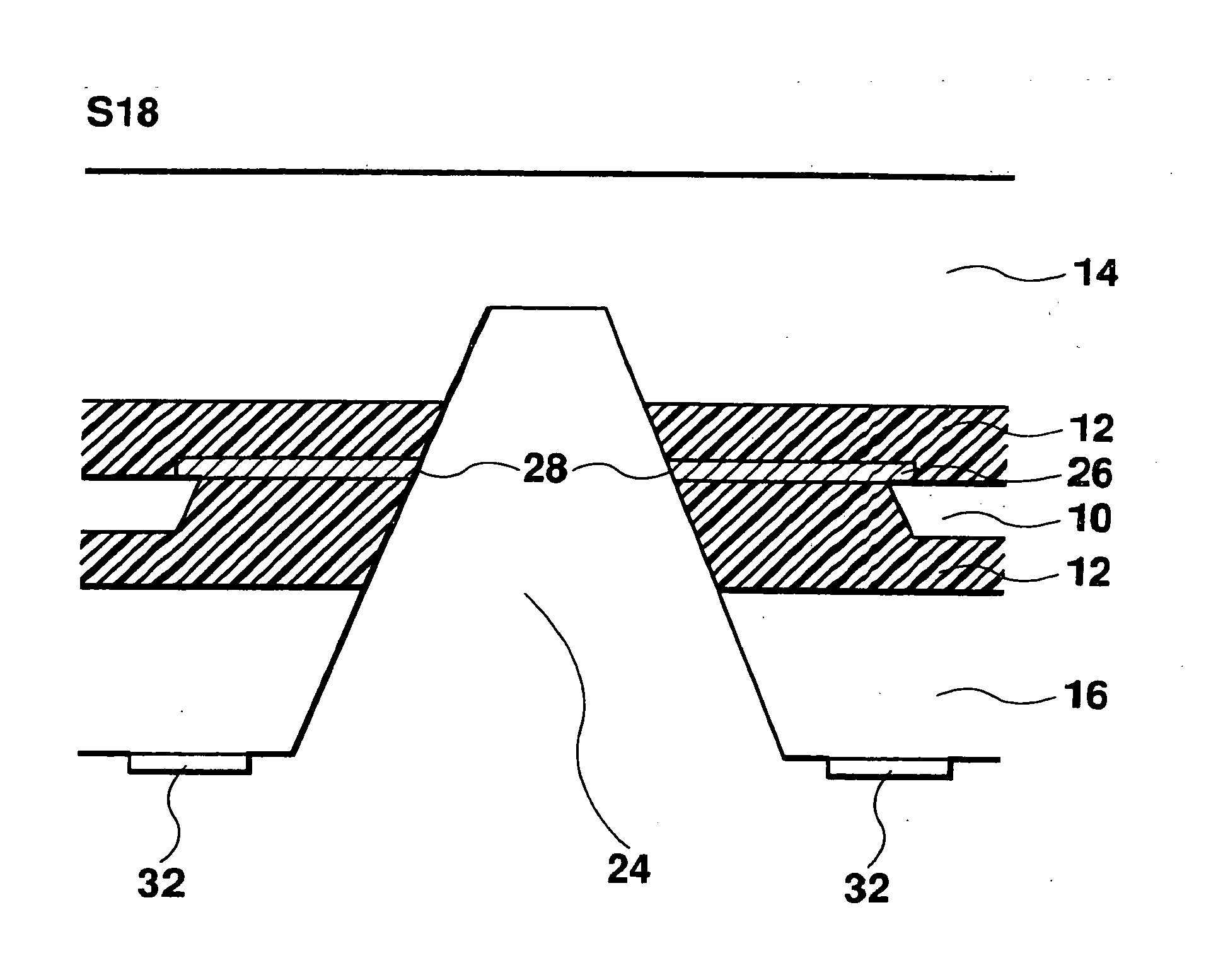
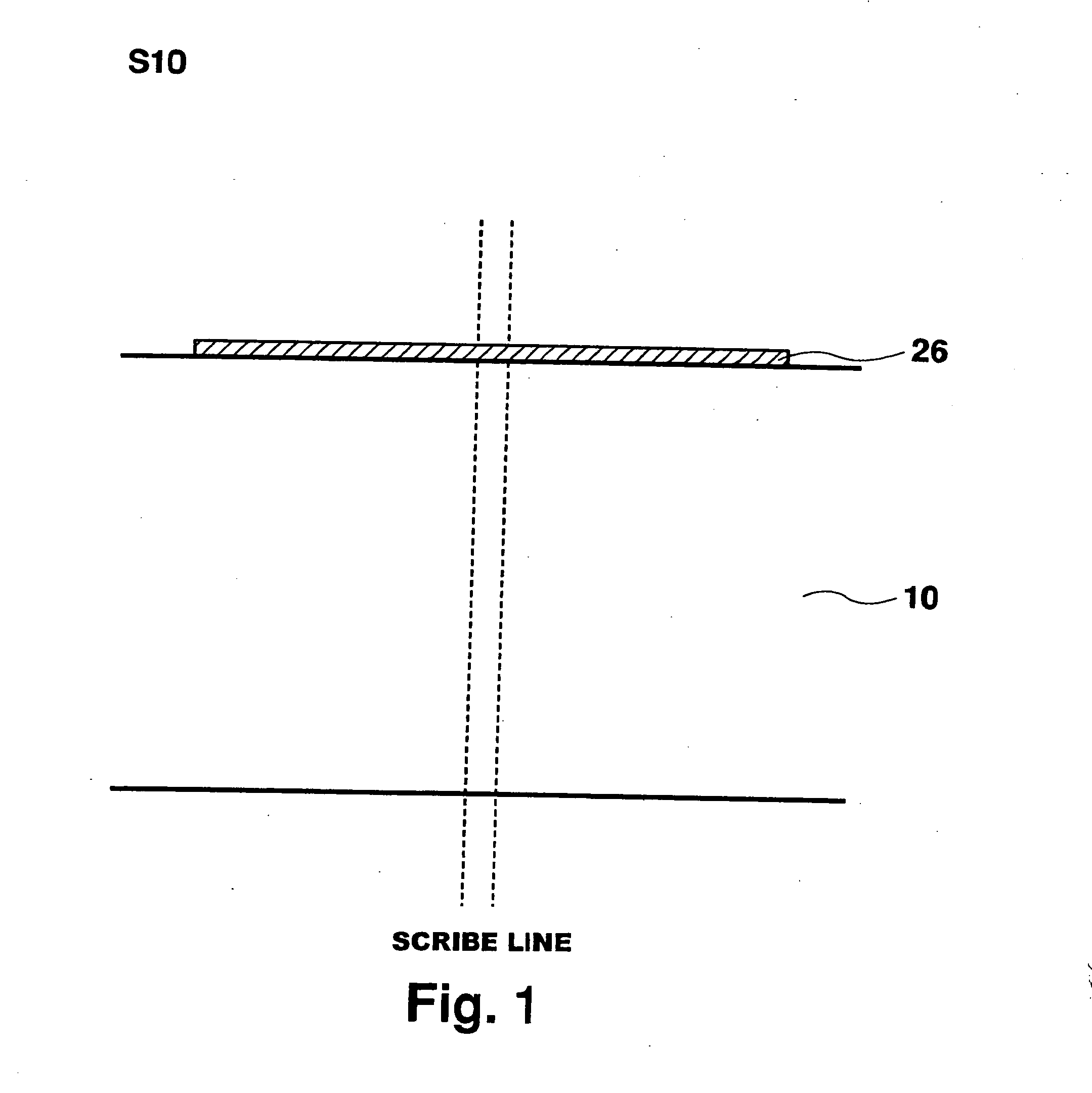
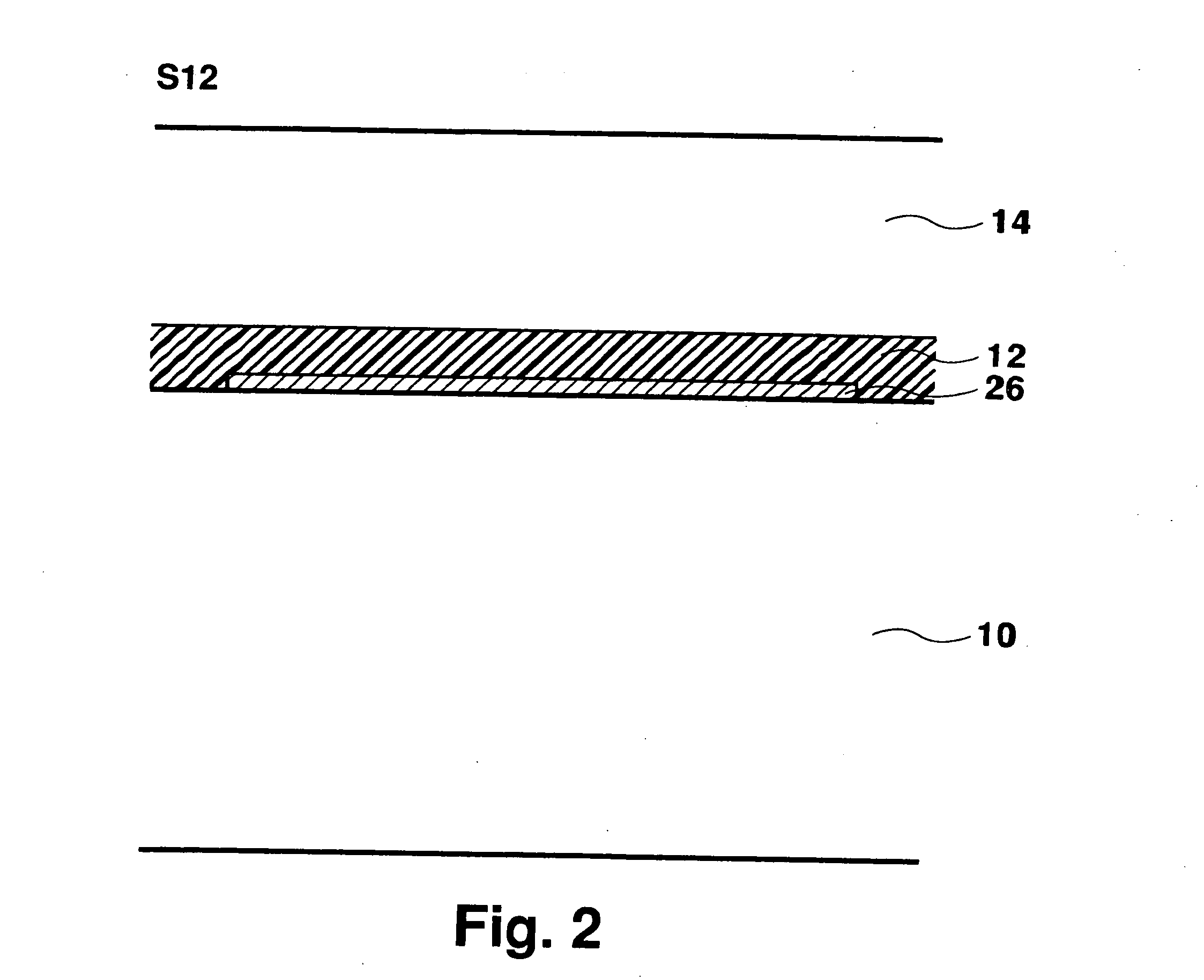
[0022] A method for manufacturing a semiconductor device according to an embodiment of the present invention comprises, as illustrated in FIGS. 1 to 8, formation of an integrated circuit element and an internal wire (S10), formation of a first laminated body (S12), grinding (S14), formation of a second laminated body (S16), cutting (S18), formation of a metal film (S20), formation of a terminal (S22), and dicing (S24).

[0023] At the step S10 for formation of an integrated circuit element and an internal wire, as shown in FIG. 1, an integrated circuit is formed in each region defined by a scribe line on the front surface of a semiconductor chip 10. Thereafter, an internal wire 26 is formed, via an oxide film, so as to extend toward the boundary relative to an adjacent integrated circuit element. The internal wire 26 is electrically connected to the associated integrated circuit element via a contact hole formed throughout the oxide film.

[0024] The semiconductor substrate 10 can be m...


PUM


Abstract

An internal wire is formed via an oxide film on the front surface of a semiconductor substrate so as to extend toward the boundary relative to an adjacent integrated circuit region. An upper supporting base is fixedly formed on the front surface of the semiconductor substrate by means of a resin layer of epoxy adhesive or the like, and a lower supporting base is fixedly formed on the back surface of the semiconductor substrate by means of a resin layer of epoxy adhesive or the like, whereby a laminated body is formed. The resin layer and the internal wire are partially removed, leaving a portion of the laminated body, to thereby form an inverted-V shaped groove (a cut-off groove) where a part of the internal wire is exposed to the outside. Thereafter, the resulting cut-off groove is exposed to plasma atmosphere to thereby dissolve, and thus remove, any remaining resin fragments attached to the exposed end portion of the internal wire.

Description

CROSS-REFERENCE TO RELATED APPLICATIONS [0001] The priority application Number No.2003-162408 upon which this patent application is based is hereby incorporated by reference. FIELD OF THE INVENTION [0002] The present invention relates to a method for manufacturing a semiconductor device which contains a laminated internal wire and resin layers. DESCRIPTION OF THE RELATED ART [0003] In recent years, chip size packages (CSP) have come to be widely used in order to reduce the size of chips for semiconductor devices. [0004]FIGS. 11A and 11B show external appearance of upper and lower surfaces of a semiconductor device utilizing a chip size package. A semiconductor integrated device utilizing a chip size package is generally constructed such that a semiconductor chip 10 is sandwiched via resin layers 12 of epoxy or the like between an upper supporting base 14 and a lower supporting base 16, with an outside wire 30 extending from the lateral side of the resultant body to be connected to a...

Claims


Application Information

Patent Timeline
Patent Type & Authority Applications(United States)
IPC IPC(8): H01L23/52H01L21/00H01L21/301H01L21/3205H01L21/44H01L21/46H01L21/70H01L21/768H01L21/78H01L23/12H01L23/31H01L23/485
CPCH01L21/76898H01L23/3114H01L24/13H01L24/10H01L2224/13099H01L2924/01004H01L2924/01013H01L2924/01022H01L2924/01029H01L2924/01033H01L2924/01073H01L2924/01074H01L2924/01079H01L2924/09701H01L2924/10329H01L2924/14H01L2924/01006H01L2924/01023H01L2924/01047H01L2924/014H01L2924/00H01L24/02H01L24/03H01L24/05H01L24/11H01L2224/02371H01L2224/02377H01L2224/05001H01L2224/05008H01L2224/05024H01L2224/05124H01L2224/05139H01L2224/05144H01L2224/05147H01L2224/05155H01L2224/05166H01L2224/05181H01L2224/05184H01L2224/05548H01L2224/05569H01L2224/05624H01L2224/05639H01L2224/05644H01L2224/05647H01L2224/05655H01L2224/05666H01L2224/05681H01L2224/05684H01L2224/06135H01L2224/13H01L2224/13024H01L2924/0001H01L2924/00014H01L2224/02
Inventor SUZUKI, NOBUHIROIMAI, KENJI
Owner SANYO ELECTRIC CO LTD
Why Eureka
Try Eureka