Piezoelectric body manufacturing method, piezoelectric body, ultrasonic probe, ultrasonic diagnosing device, and nondestructive inspection device

a manufacturing method and piezoelectric technology, applied in the field of piezoelectric/electrostrictive device details, instruments, applications, etc., can solve the problems of uneven thickness of piezoelectric devices, easy cracking of piezoelectric devices, and conventional ultrasonic probes, etc., to achieve high precision, reliably operate, and high reliability

Inactive Publication Date: 2005-01-20
PANASONIC CORP
View PDF10 Cites 4 Cited by
  • Summary
  • Abstract
  • Description
  • Claims
  • Application Information

AI Technical Summary

Benefits of technology

[0021] (d) fixedly connecting the first piezoelectric body to the second piezoelectric body with the second surface of the first piezoelectric body held in contact with the first surface of the second piezoelectric body. The present invention makes it possible for a manufacturer to produce a piezoelectric device having a predetermined uneven thickness distribution with ease, while eliminating the need of carrying out any technically-difficult minute machining processing such as for example a grinding processing, thereby resulting in the fact the piezoelectric device is kept from being excessively distorted so that the piezoelectric device is not cracked. In addition, the present invention makes it possible for a manufacturer to constantly produce a plurality of piezoelectric devices equal in shape to one another with high precision because of the fact that the shape of the die is simply transferred to them, thereby resulting in the fact the piezoelectric device thus produced can reliably operate without being influenced by differences among piezoelectric devices. The piezoelectric device having electrodes spaced apart from each other at a constant distance although the piezoelectric device has an uneven thickness distribution can maintain its polarization state constant, thereby ensuring that ultrasonic waves are transmitted and received with high reliability.
[0022] In accordance with the present invention, there is provided an ultrasonic diagnostic apparatus equipped with an ultrasonic probe comprising a piezoelectric device having a construction produced through the steps of: (c) producing a first piezoelectric body having a non-plane first surface and a plane second surface opposite to the first surface, and a second piezoelectric body having a plane first surface and a plane second surface opposite to the first surface, the second piezoelectric body having electrodes respectively on the first and second surfaces; and (d) fixedly connecting the first piezoelectric body to the second piezoelectric body with the second surface of the first piezoelectric body held in contact with the first surface of the second piezoelectric body. The ultrasonic probe thus constructed has an advantage of stably operating without being influenced by differences among piezoelectric devices. The ultrasonic diagnostic apparatus thus constructed can carry out an ultrasound diagnosis with high reliability, taking the advantage of the ultrasonic probe.
[0023] In accordance with the present invention, there is provided a nondestructive testing apparatus equipped with an ultrasonic probe comprising a piezoelectric device having a construction produced through the steps of: (c) producing a first piezoelectric body having a non-plane first surface and a plane second surface opposite to the first surface, and a second piezoelectric body having a plane first surface and a plane second surface opposite to the first surface, the second piezoelectric body having electrodes respectively on the first and second surfaces; and (d) fixedly connecting the first piezoelectric body to the second piezoelectric body with the second surface of the first piezoelectric body held in contact with the first surface of the second piezoelectric body. The ultrasonic probe thus constructed has an advantage of stably operating without being influenced by differences among piezoelectric devices. The nondestructive testing apparatus thus constructed can carry out a nondestructive test with high reliability, taking the advantage of the ultrasonic probe.

Problems solved by technology

The conventional ultrasonic probe as previously mentioned, however, encounters a drawback that the piezoelectric device is quite easy to be cracked by the reason that the thickness of the piezoelectric device is required to be several hundred μm in the case that the conventional ultrasonic probe is for use in, for example, an ultrasonic diagnostic apparatus, and the piezoelectric device is designed to emit an ultrasonic wave of several MHz, and made of a ground piezoelectric ceramic such as for example PZT (lead zirconate titanate).
The conventional ultrasonic probe encounters another drawback that a distance between electrodes respectively placed on a first surface of the piezoelectric device and a second surface of the piezoelectric device opposite to the first surface of the piezoelectric device across the thickness of the piezoelectric device tends to be uneven by the reason that the thickness of the piezoelectric device constituting the conventional ultrasonic probe is uneven.
The unevenness of the distance between the electrodes causes electric field strength and thus polarization state to be uneven in the event that a power voltage is applied to the piezoelectric device to polarize the piezoelectric device.
The fact that an electric field applied to the thin center portion is greater than an electric field applied to the end portion while the piezoelectric device is polarized leads to the fact that the piezoelectric device is caused to be distorted, thereby making it easier for the piezoelectric device to be cracked while the piezoelectric device is polarized.
Furthermore, the fact that the electric field applied to the thin center portion is greater than the electric field applied to the end portion while the piezoelectric device is driven leads to the fact that the piezoelectric device is caused to be distorted, thereby making it easier for the piezoelectric device to be cracked while the conventional ultrasonic probe is driven.
The conventional method of producing a piezoelectric device encounters a drawback that a thin portion of the piezoelectric device is difficult to be ground by the reason that the conventional method comprises the step of carrying out a grinding processing on materials of the piezoelectric device.
As the ultrasonic diagnostic apparatus is required to emit an ultrasonic wave of a higher frequency such as, for example, several dozen MHz, it becomes more difficult to grind the thin portion of the piezoelectric device.
Assuming that the thickness of the piezoelectric device is several hundred μm at the end portion, a grinding tool such as, for example, a grinding wheel 5 is required to be minute in size equal to or less than several hundred μm, and it is extremely difficult to carry out a grinding processing on materials of the piezoelectric device.
It is also extremely difficult to constantly produce a plurality of piezoelectric devices equal in shape to one another with high precision.

Method used


Image

  • Piezoelectric body manufacturing method, piezoelectric body, ultrasonic probe, ultrasonic diagnosing device, and nondestructive inspection device
  • Piezoelectric body manufacturing method, piezoelectric body, ultrasonic probe, ultrasonic diagnosing device, and nondestructive inspection device
  • Piezoelectric body manufacturing method, piezoelectric body, ultrasonic probe, ultrasonic diagnosing device, and nondestructive inspection device

Examples


first embodiment

[0052] [First Embodiment]

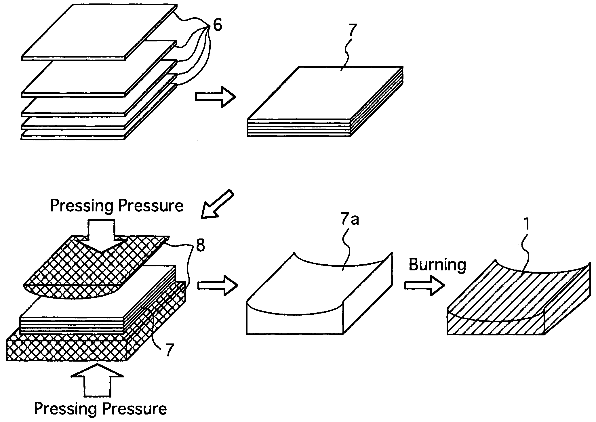
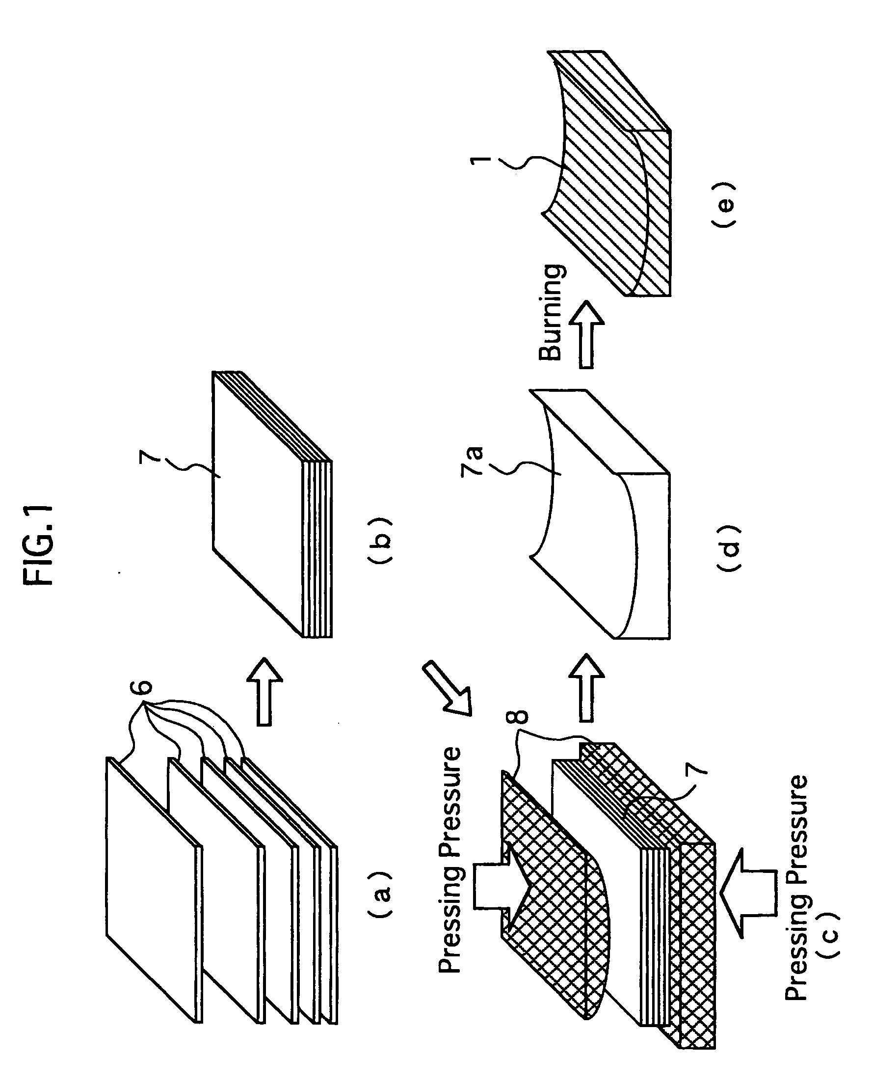
[0053] Referring now to FIG. 1 of the drawings, there is shown a first preferred embodiment of a method of producing a piezoelectric device 1, comprising: molding and laminating processes (first step (a)) of molding one or more raw material elements 6 including at least one piezoelectric material to form a predetermined piezoelectric element 7 (raw piezoelectric element); and a pressing process (second step (b)) imparting pressing forces to the piezoelectric element 7 to have the piezoelectric element 7 molded into a predetermined shape.

[0054] The present embodiment of the piezoelectric device 1 has a plane first surface and a concave second surface opposite to the first surface. The second surface has a thickness concavely curved in a manner that the thickness of the second surface gradually increases from a center portion toward end portions. The piezoelectric device 1 in part constitutes an ultrasonic probe (shown FIG. 20) to be used for an ultrasonic di...

second embodiment

[0067] [Second Embodiment]

[0068] Referring then to FIG. 3 of the drawings, there is shown a second preferred embodiment of a method of producing a piezoelectric device 1. The present embodiment of the producing method is different from the first embodiment of the producing method in the fact that the molding and laminating process (first step (a)) further has a process of laminating a plurality of raw material elements 6 (sheet-like raw material elements) respectively having thicknesses collectively in accordance with a thickness distribution of the piezoelectric device. Preferably, the shape and the number of sheet-like raw material elements 6 to be laminated should be calculated in accordance with the thickness distribution of the piezoelectric device 1. The present embodiment of the producing method has an additional effect of being capable of producing a piezoelectric device 1 having a predetermined thickness distribution with increased flexibility by adaptively laminating a plu...

third embodiment

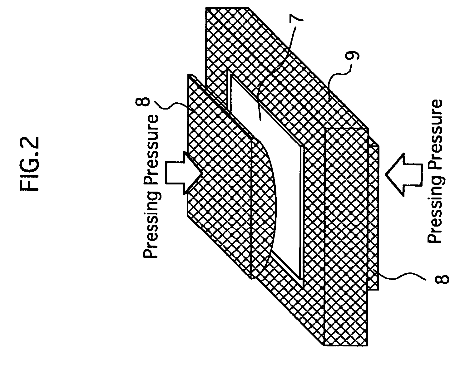
[0080] [Third Embodiment]

[0081] Referring then to FIG. 5 of the drawings, there is shown a third preferred embodiment of a method of producing a piezoelectric device 1. The present embodiment of the producing method is different from the first embodiment of the producing method in the fact that the molding and laminating process (first step (a)) further has a process of laminating one or more raw material elements respectively formed with through bores in accordance with a thickness distribution of the piezoelectric device 1. The present embodiment of the producing method has an additional effect of being capable of producing a piezoelectric device 1 having a predetermined shape and thickness distribution with increased flexibility.

[0082] The present embodiment of the piezoelectric device 1 has a plane first surface and a concave second surface opposite to the first surface. The second surface has a thickness concavely curved in a manner that the thickness of the second surface gra...


PUM

PropertyMeasurementUnit
thicknessaaaaaaaaaa
thicknessaaaaaaaaaa
thicknessaaaaaaaaaa

Abstract

Herein disclosed are a piezoelectric device, an ultrasonic probe, an ultrasonic diagnostic apparatus, a nondestructive testing device, and a method of producing one or more piezoelectric devices respectively having predetermined thickness distributions equal in shape to one another with high precision to realize an ultrasound diagnosis with high reliability. The method of producing one or more piezoelectric devices comprises a molding process of: molding a mixture of raw materials including piezoelectric ceramic powders and a binding agent immersed in a solvent to form a plurality of sheet-like raw material elements 6 each having a thickness in a range of a few ten microns to a few hundred microns by way of, for example, a Doctor Blade technique, a laminating process of laminating a plurality of sheet-like raw material elements 6 to obtain a piezoelectric element 7, a pressing process of imparting pressing forces to the piezoelectric element 7 to obtain a piezoelectric element 7a having a predetermined shape, and a burning process of burning the piezoelectric element 7a.

Description

TECHNICAL FIELD [0001] The present invention relates to a method of producing a piezoelectric device available for diagnosis, treatment, nondestructive testing, or the like, and more particularly to a piezoelectric device, an ultrasonic probe, an ultrasonic diagnostic apparatus, and a nondestructive testing device. BACKGROUND ART [0002] The conventional ultrasonic probe of this type is shown in FIG. 24 as comprising a piezoelectric device 1 having a thickness concavely curved in a manner that the thickness of the piezoelectric device 1 gradually increases from a center portion toward end portions along the minor axis, an acoustic matching layer 2 having a thickness concavely curved in accordance with that of the piezoelectric device 1 with a result that the thickness of the acoustic matching layer 2 gradually increases from a center portion toward end portions along the minor axis to ensure that an ultrasonic wave is efficiently transmitted and received, an acoustic lens 3 for conve...

Claims


Application Information

Patent Timeline
Patent Type & Authority Applications(United States)
IPC IPC(8): A61B8/00G01N29/24H04R17/00H04R31/00
CPCH04R17/00H01L41/297H01L41/293H01L41/273H10N30/067H10N30/063H10N30/053
Inventor SATO, TOSHIHARUAMEMIYA, KIYOHIDESUGIYAMA, YOSHIYUKI
Owner PANASONIC CORP
Why Eureka
Try Eureka