

Electro-optical apparatus and electronic system
- Summary
- Abstract
- Description
- Claims
- Application Information
AI Technical Summary
Benefits of technology
Problems solved by technology
Method used
Image

Examples
first embodiment
[0051] A description will be given of an electro-optical apparatus according to the invention with reference to FIGS. 1 to 10.
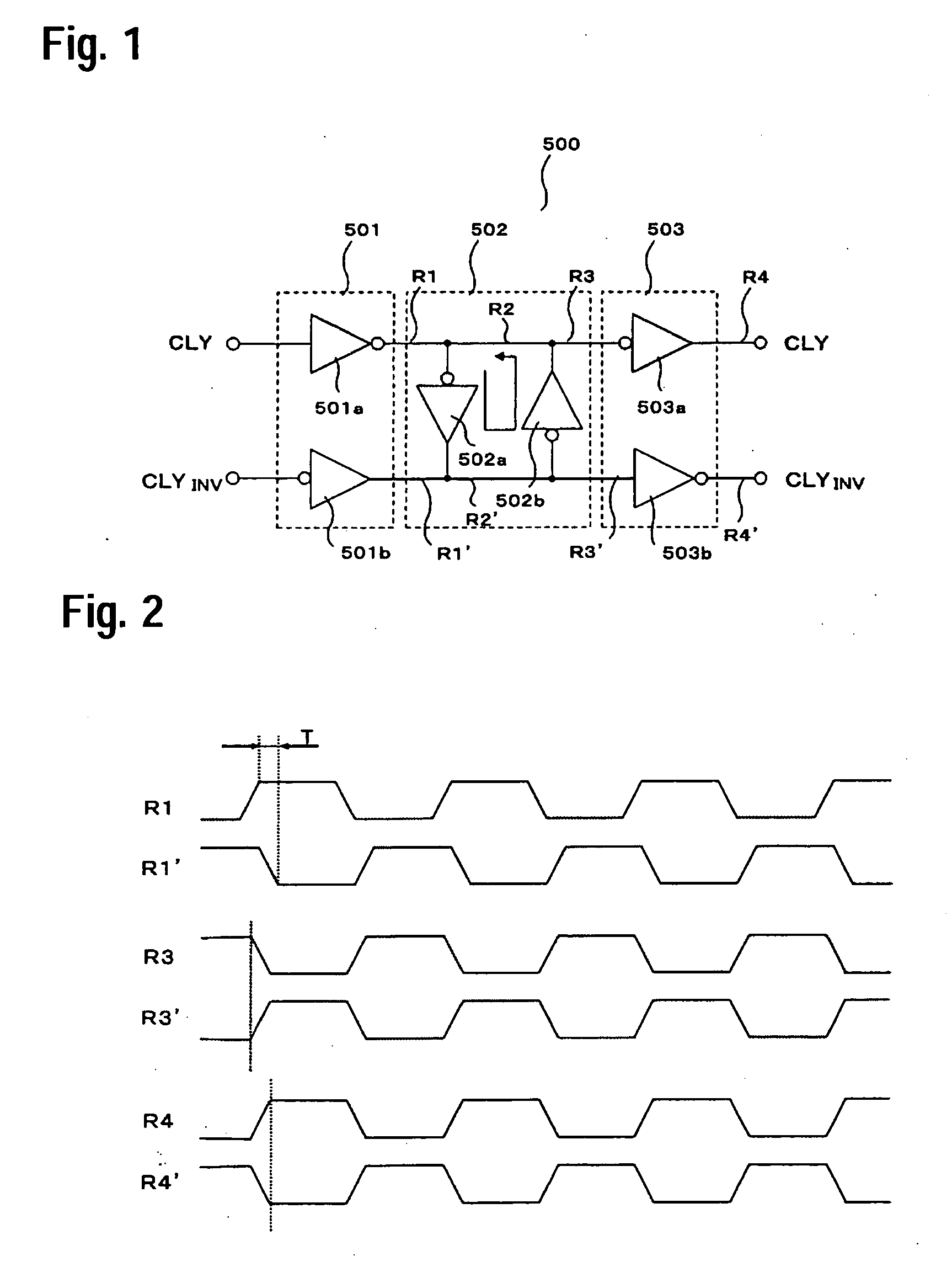
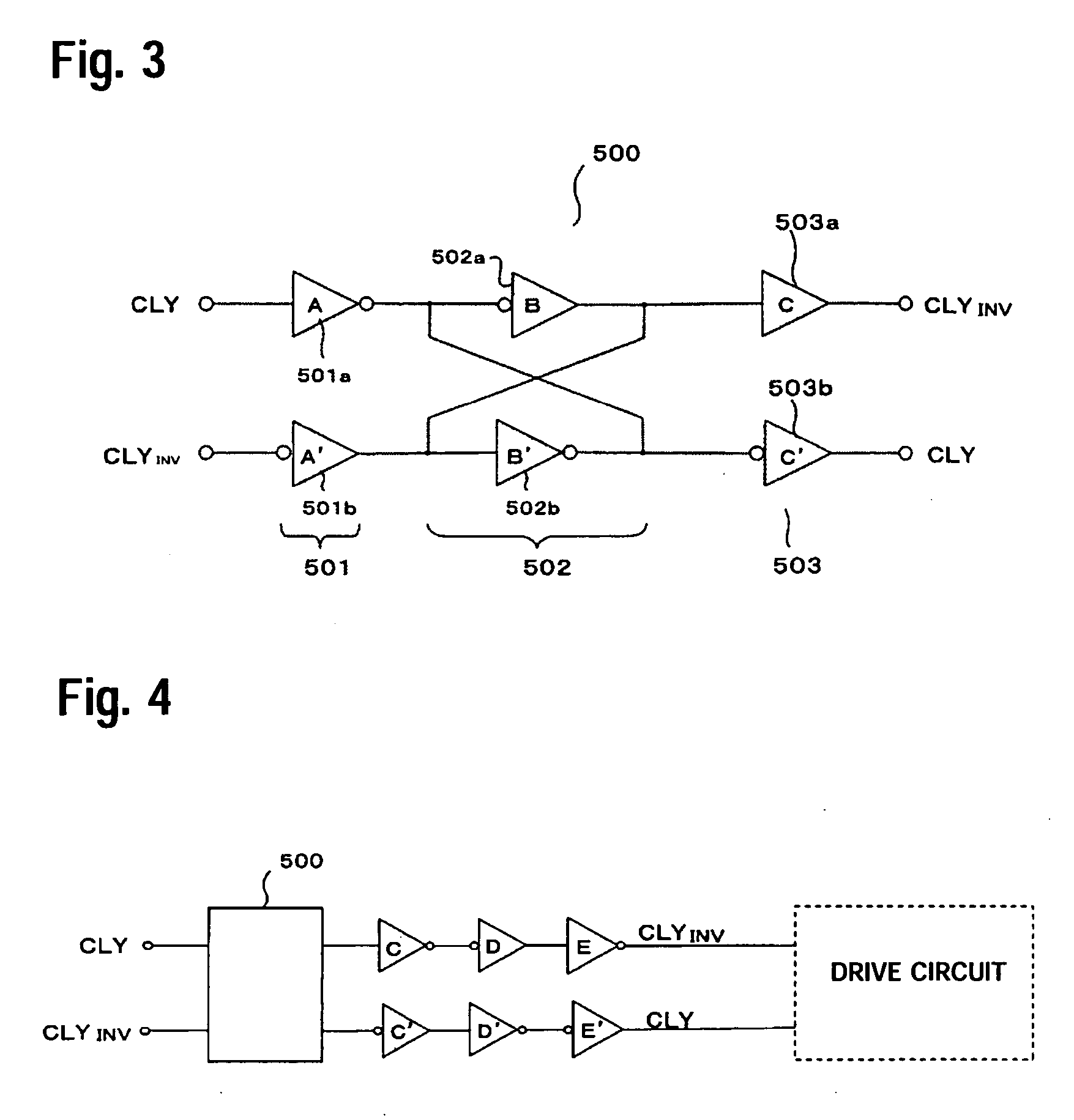
[0052] First, a description will be given of the configuration and the operation of a clock-signal phase difference correction circuit according to the embodiment with reference to FIGS. 1 to 4. Here, FIG. 1 is an exemplary circuit diagram illustrating the configuration of the clock-signal phase difference correction circuit according to the embodiment. FIG. 2 is a timing chart illustrating the time-series changes of the various signals related to the circuit. FIG. 3 is an exemplary circuit diagram for explaining the load capacitance of each signal path in the clock-signal phase difference correction circuit. FIG. 4 is an exemplary circuit diagram when a second buffer circuit includes multistage inverter circuits in the clock-signal phase difference correction circuit according to the present embodiment.
[0053] In the electro-optical apparatus of the embodime...
second embodiment
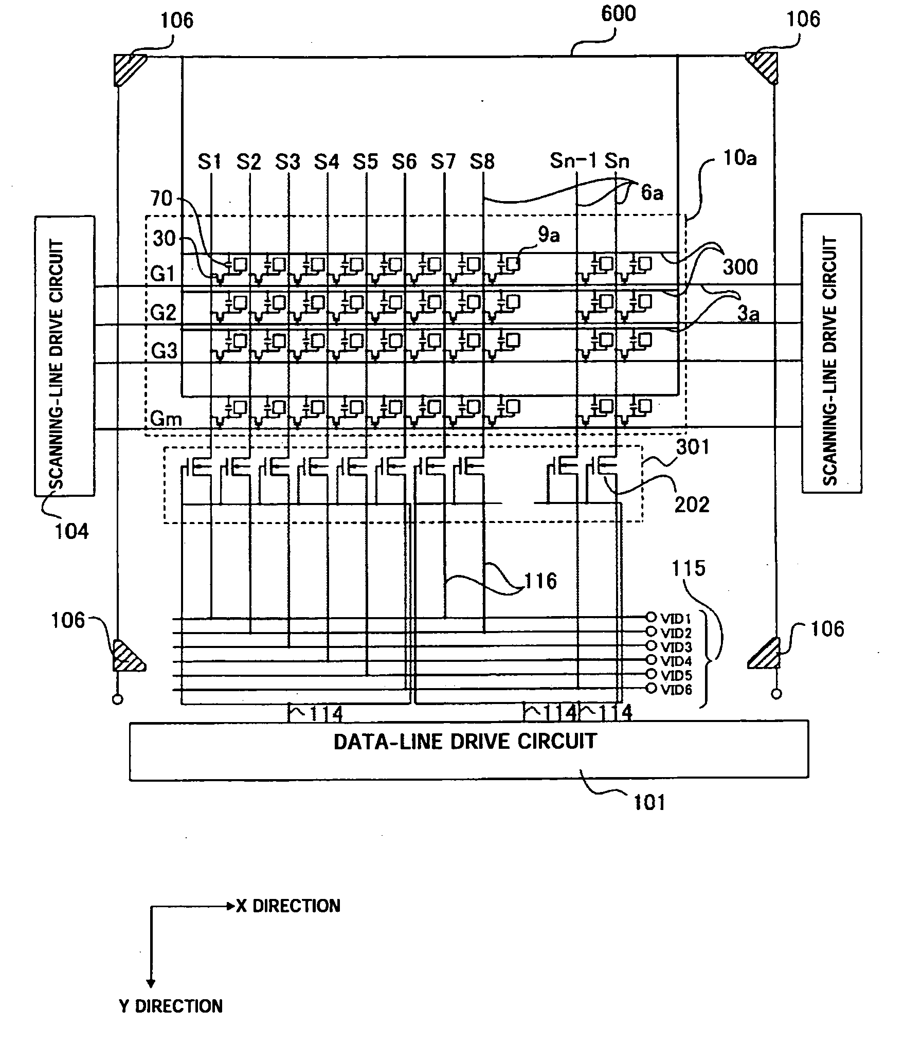
[0114] With the arrangement, the wiring line distance from the clock-signal phase difference correction circuit 500 to the scanning-line drive circuit 104R and the wiring line distance from clock-signal phase difference correction circuit 500 to the scanning-line drive circuit 104L become equal, and thus the wiring time constants of both wiring lines become equal. Thus, for example, even if signal delays occur from the clock-signal phase difference correction circuit 500 to the scanning-line drive circuit 104R and the scanning-line drive circuit 104L, the individual signal delays till the right and left scanning-line drive circuits are equal, and thus it becomes possible to prevent the trouble of the occurrence of the difference in the driving timing between the right and the left scanning-line drive circuits due to the signal delays. Furthermore, it is possible to reduce the space of the area outer than the periphery of the sealing area 52a, which is provided for the clock-signal p...
PUM
 Abstract
Description
Claims
Application Information