Image sensor with charge binning and dual channel readout

a dual-channel readout, image sensor technology, applied in the direction of picture signal generators, television system scanning details, television systems, etc., can solve the problems of image sensor design and performance, low noise column storage and readout circuits, and insufficient signal levels for low illumination levels of small pixels, so as to achieve low noise and high sensitivity multiple resolution

Active Publication Date: 2005-01-20
OMNIVISION TECH INC
View PDF31 Cites 110 Cited by
  • Summary
  • Abstract
  • Description
  • Claims
  • Application Information

AI Technical Summary

Benefits of technology

The invention has the following advantages. It provides for low noise, high sensitivity multiple resolution imaging from a single image sensor.

Problems solved by technology

As the pixel size decreases, several image sensor design and performance disadvantages are encountered.
First, it becomes increasingly more difficult to construct a low noise column storage and readout circuit.
Second, smaller pixels have lower sensitivity and can provide inadequate signal levels for low levels of illumination.
Third, for a large number of pixels, the readout time will become longer.
While this approach provides video rate data, it does so by selective readout of the small pixels and still has poor image quality in low light level environments, and produces aliasing image artifacts.
For high resolution sensors, this has the disadvantage of requiring higher performance PGAs.

Method used


Image

  • Image sensor with charge binning and dual channel readout
  • Image sensor with charge binning and dual channel readout
  • Image sensor with charge binning and dual channel readout

Examples


Embodiment Construction

The examples and diagrams provided in the description of the present invention represent one preferred embodiment of the present invention. Numerous other specific embodiments are feasible without departing from the scope of the present invention.

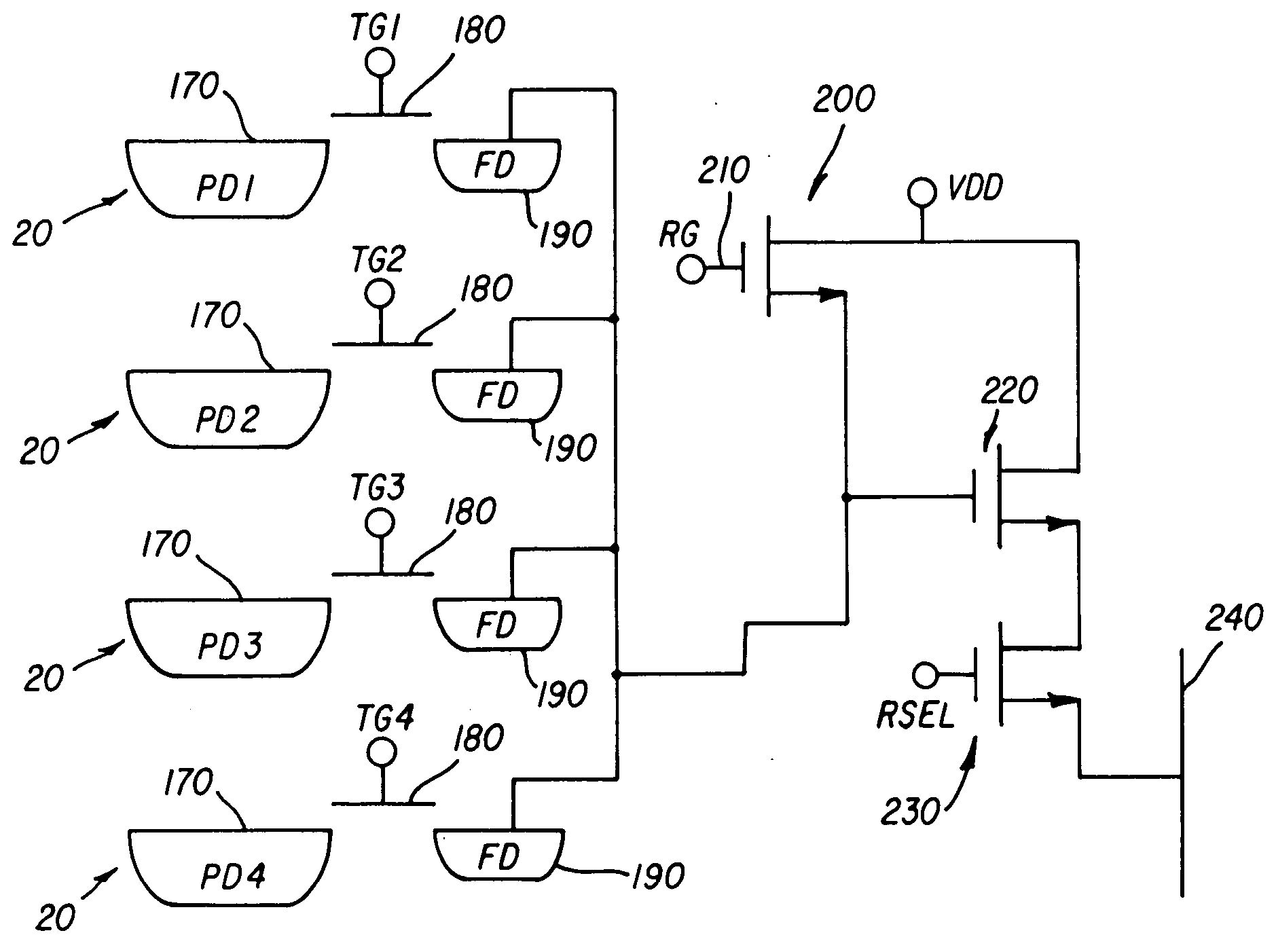
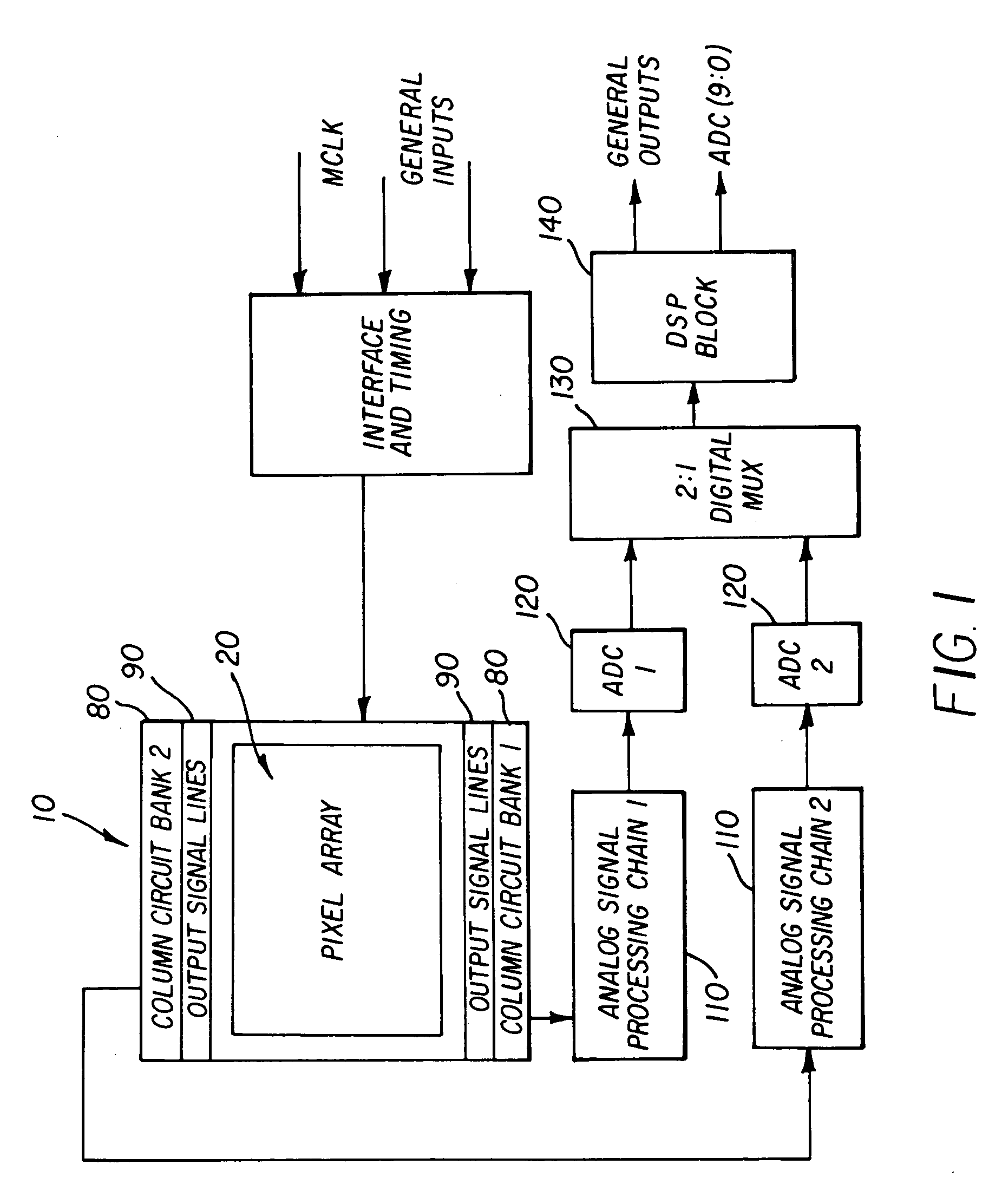
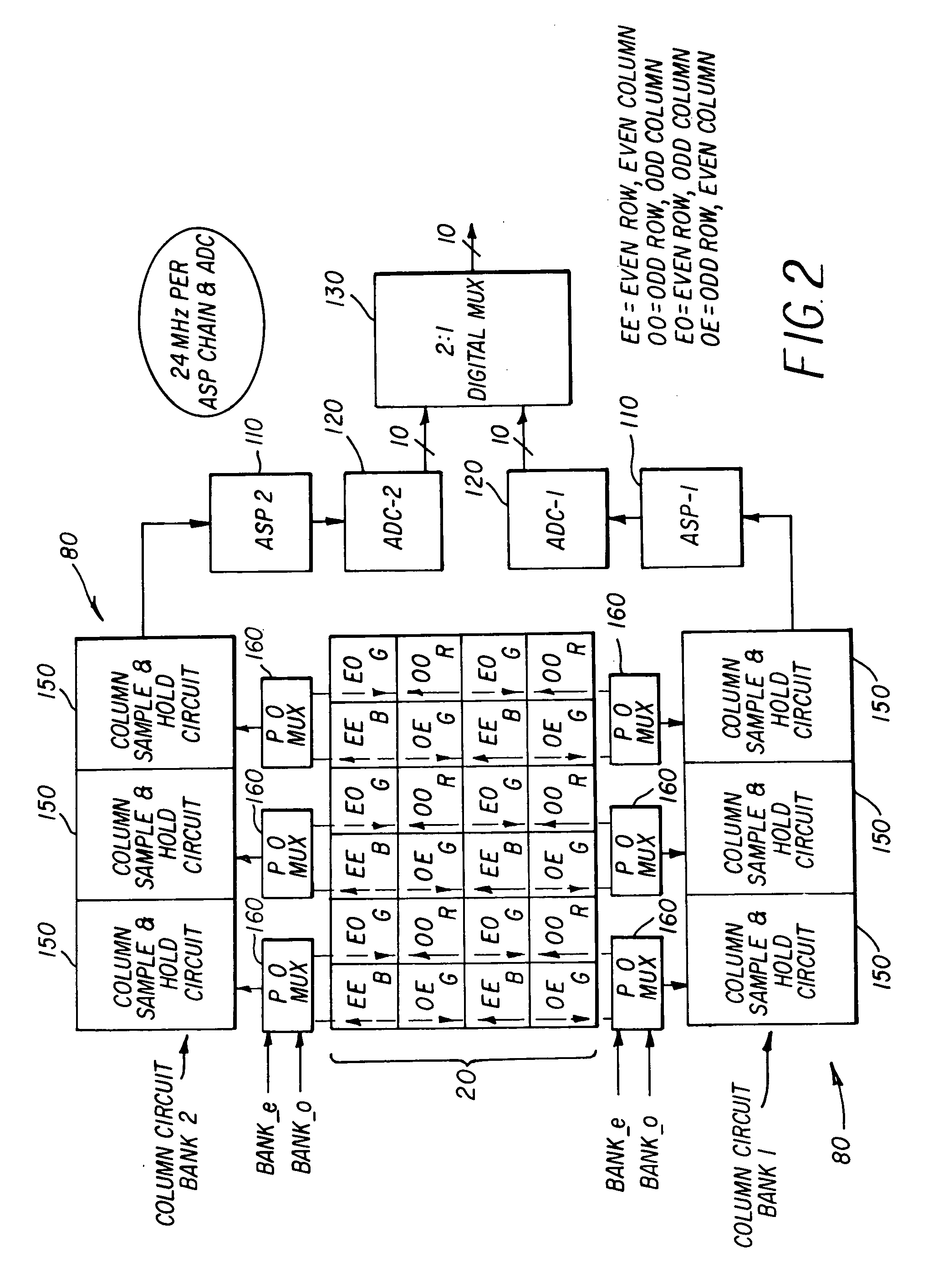
Referring to FIG. 1, there is shown a top level block diagram of the image sensor 10 of the present invention. The sensor array comprises a plurality of pixels 20. The pixels 20 can be any known APS or PPS x-y addressable pixel design. Two column circuit banks 80 (also referred to as storage regions), each comprising a plurality of column sample and hold circuits (not shown in FIG. 1) are electrically connected to the output signal lines 90 of the sensor array 10. Two parallel analog signal processing (ASP) chains 110 (also referred to as readout regions) are respectively connected to each column circuit bank 80. An analog to digital converter (ADC) 120 is electrically connected to each processing chain 110 for digitizing the signal. A 2...


PUM


Abstract

An image sensor includes: (a) a plurality of light measuring elements arranged in an array and at least a portion of the elements have a color filter mated with the light receiving elements which permits selective color reception by the light measuring elements; (b) a plurality of floating diffusions respectively mated with the plurality of light receiving elements; and c) an output structure electrically connected to two or more of the floating diffusions; wherein the at least two light receiving elements receiving the same color are transferred to the output structure substantially simultaneously.

Description

FIELD OF THE INVENTION The present invention pertains to semiconductor based image sensors such as Active Pixel image sensors (APS), and Passive Pixel image sensors (PPS), and more particularly, to such APS and PPS with charge binning, high sensitivity, low noise, and parallel channel readout. BACKGROUND OF THE INVENTION APS and PPS are x-y addressable solid state imagers wherein each pixel contains both a photosensing element and a select element. For APS, each pixel also contains at least one other active circuit component. In both APS and PPS, incident illumination is converted to a signal (either a voltage or current signal). The signal represents the amount of light incident upon a pixel photosite. This signal is typically readout one row at time, and the signals for a given row are stored temporarily in a circuit associated with each column of the image sensor. This column circuit is typically constructed to fit into the size or pitch of the pixel. For many digital imaging ...

Claims


Application Information

Patent Timeline
Patent Type & Authority Applications(United States)
IPC IPC(8): H04N5/347H04N5/357H04N5/378H04N9/04H04N9/07
CPCH04N3/1562H04N9/045H04N5/347H04N25/46H04N25/767H04N25/70H04N23/84H04N25/134H04N25/77H04N25/75
Inventor GUIDASH, ROBERT M.
Owner OMNIVISION TECH INC
Why Eureka
Try Eureka