Semiconductor integrated circuit for communication

a technology of integrated circuits and semiconductors, applied in the field of semiconductor integrated circuits for communication, can solve problems such as difficulty in achieving large output amplitudes, and achieve the effects of preventing reception signals, preventing noise characteristics from deteriorating, and avoiding noise figures (nf) of the whole reception circuitry

Inactive Publication Date: 2005-01-20
RENESAS ELECTRONICS CORP
View PDF8 Cites 39 Cited by
  • Summary
  • Abstract
  • Description
  • Claims
  • Application Information

AI Technical Summary

Benefits of technology

[0015] As the means described above can prevent the output signal of the LNA of the selected band from leaking into the output of the LNAs of unselected bands, and thereby preventing inviting a drop in the output level of the LNA of the selected band, a deterioration in noise figure (NF) of the whole reception circuitry can be avoided.
[0016] Preferably, where the low noise amplifier (LNA) of each band is of a differential type, a switching element

Problems solved by technology

Resistors, if used as the output load on the orthogonal modulating circuit, would invite a voltage drop and narro

Method used


Image

  • Semiconductor integrated circuit for communication
  • Semiconductor integrated circuit for communication
  • Semiconductor integrated circuit for communication

Examples


Embodiment Construction

[0030] Next will be described preferred embodiments of the present invention with reference to the accompanying drawings.

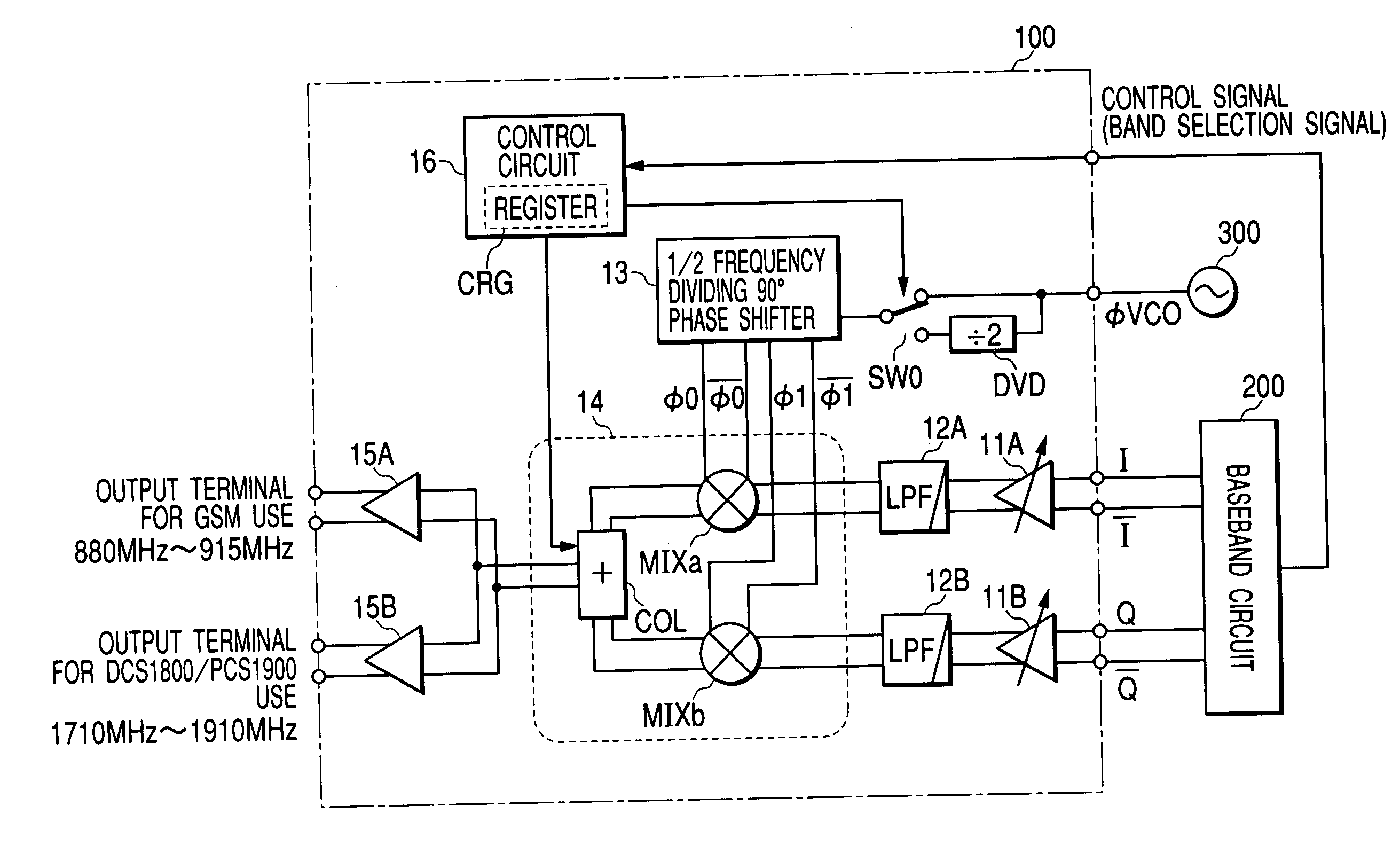
[0031]FIG. 1 shows a first preferred embodiment of the invention, which is a transmission circuitry of a direct up conversion formula.

[0032] In FIG. 1, reference numeral 100 denotes a semiconductor integrated circuit for communication use (hereinafter referred to as a modulating / demodulating LSI) in the transmission circuitry embodying the invention; 200, a baseband circuit; and 300, a local voltage control oscillator (VCO) generating a local oscillation signal. The baseband circuit 200 converts transmission data into I signals and Q signals and supplies them to the modulating / demodulating LSI 100, and generates control signals for the modulating / demodulating LSI 100. It consists of one or a few semiconductor integrated circuits (IC). The I and Q signals may be, though not necessarily are, supplied as differential signals I, / I, Q and / Q to the modulating / demodu...


PUM


Abstract

An orthogonal modulating circuit for modulating signals of two oscillation frequencies differing in phase by 90° with transmission data (I and Q) is used in common for a plurality of bands, an LC resonance circuit comprising inductances L and a capacitor C is used as the output load on the orthogonal modulating circuit instead of resistors commonly used according to the prior art, and the values of L or C constituting the resonance circuit are switched over between each other according to the transmission band.

Description

CROSS-REFERENCE TO RELATED APPLICATION [0001] The present application claims priority from Patent Cooperation Treaty patent application PCT / JP02 / 010715 filed on Oct. 16, 2002, the content of which is hereby incorporated by reference into this application.TECHNICAL FIELD [0002] The present invention relates to a technique that can be effectively applied to a semiconductor integrated circuit for communication for use in wireless communication apparatuses of a direct conversion formula, and more particularly to a technique that can be effectively applied to a modulating circuit and a demodulating circuit constituting a cellular phone or the like that can transmit and receive signals of a plurality of bands. BACKGROUND ART [0003] For a communication apparatus, such as a cellular phone, reductions not only in size and weight but also in cost are keenly called for. This cost saving can be effectively accomplished by reducing such external parts as a voltage control oscillator (VCO) and a ...

Claims


Application Information

Patent Timeline
IPC IPC(8): H03C3/40H04B1/04H04B1/30H04B1/40H04L27/00H04L27/20H04L27/32H04L27/36
CPCH03C3/40H04B1/005H04B1/04H04B1/0458H04L2027/0016H04B1/406H04L27/2064H04L27/32H04L27/362H04B1/30
Inventor OONO, MASACHIKAMATSUI, HIROAKIYAHAGI, KOICHI
Owner RENESAS ELECTRONICS CORP
Why Eureka
Try Eureka