Wafer-level burn-in and test

Inactive Publication Date: 2005-01-27
FORMFACTOR INC
View PDF85 Cites 17 Cited by
  • Summary
  • Abstract
  • Description
  • Claims
  • Application Information

AI Technical Summary

Benefits of technology

[0054] An advantage of the invention is that DUT operation can be ascertained over a wide temperature range, from well below room temperature to the maximum temperature allowed by the semiconductor process, all without thermally stressing t

Problems solved by technology

Due to defects in the wafer, or to defects in one or more of the processing steps, certain ones of the semiconductor devices will not function as designed, these defects may show up initially or may not be appare

Method used


Image

  • Wafer-level burn-in and test
  • Wafer-level burn-in and test
  • Wafer-level burn-in and test

Examples


Embodiment Construction

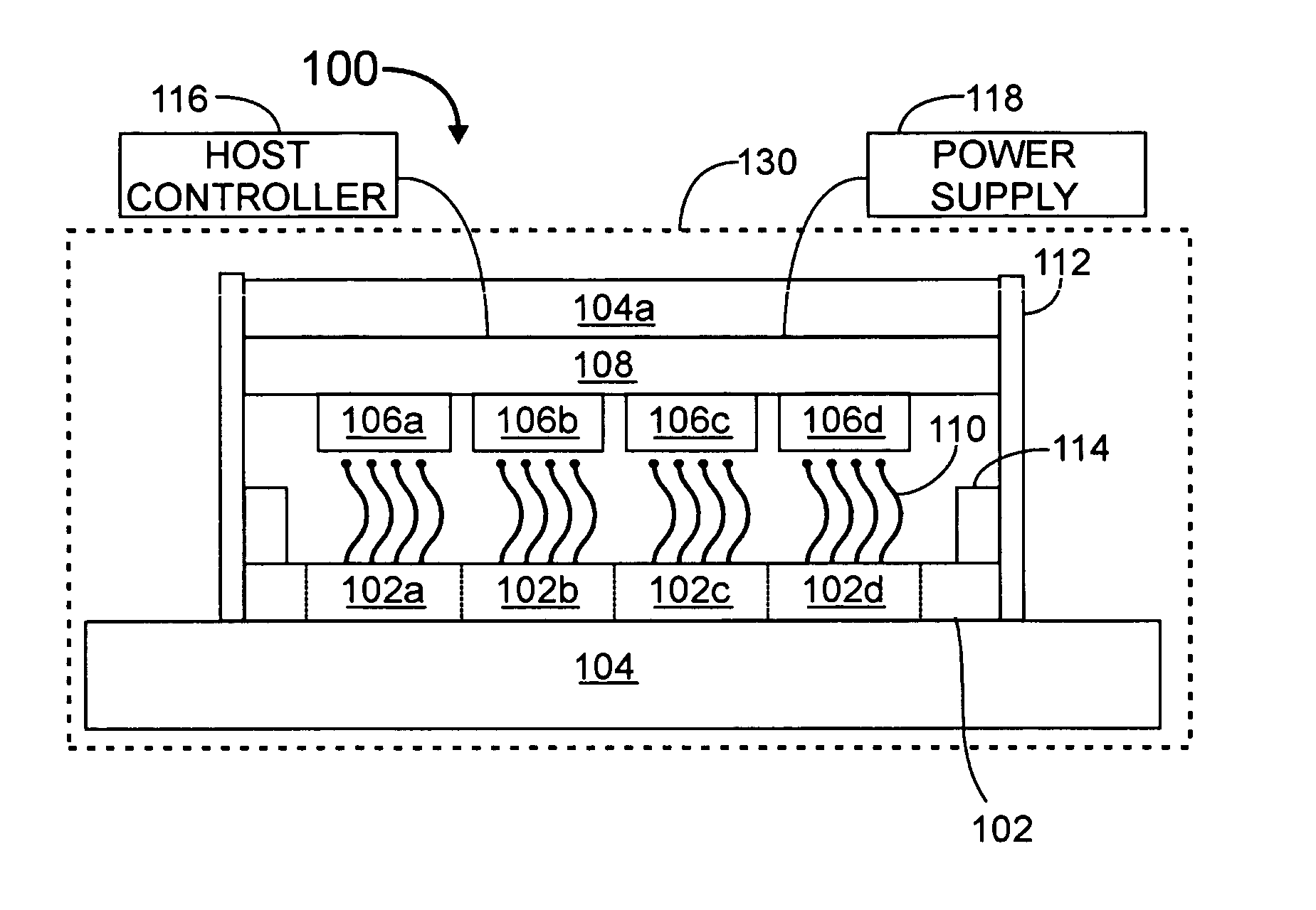
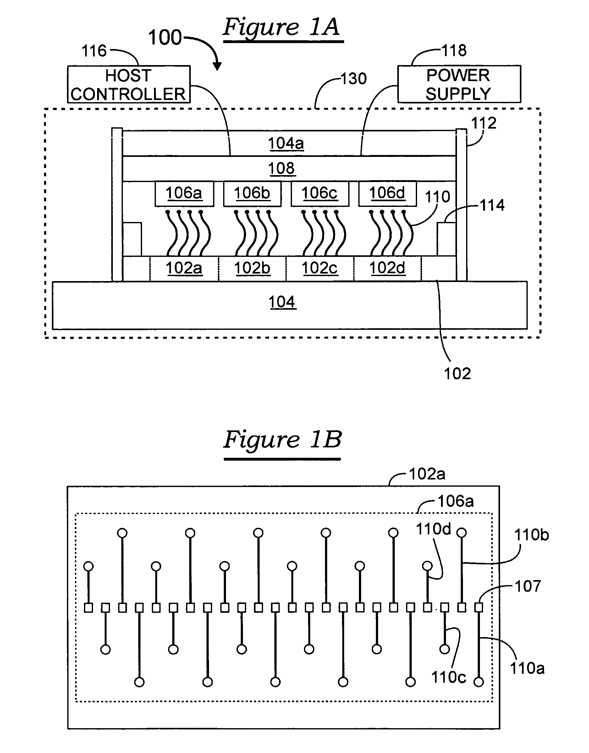
[0073]FIG. 1A illustrates an apparatus 100 for performing a method of wafer-level burn-in and test, according to the invention. A wafer under test (WUT) is disposed (received) on a suitable support, such as a temperature-controlled vacuum chuck 104, such that the semiconductor devices 102a, 102b, 102c, 102d formed on the WUT (the WUT is generally referred to herein as element 102) are facing up (as viewed).

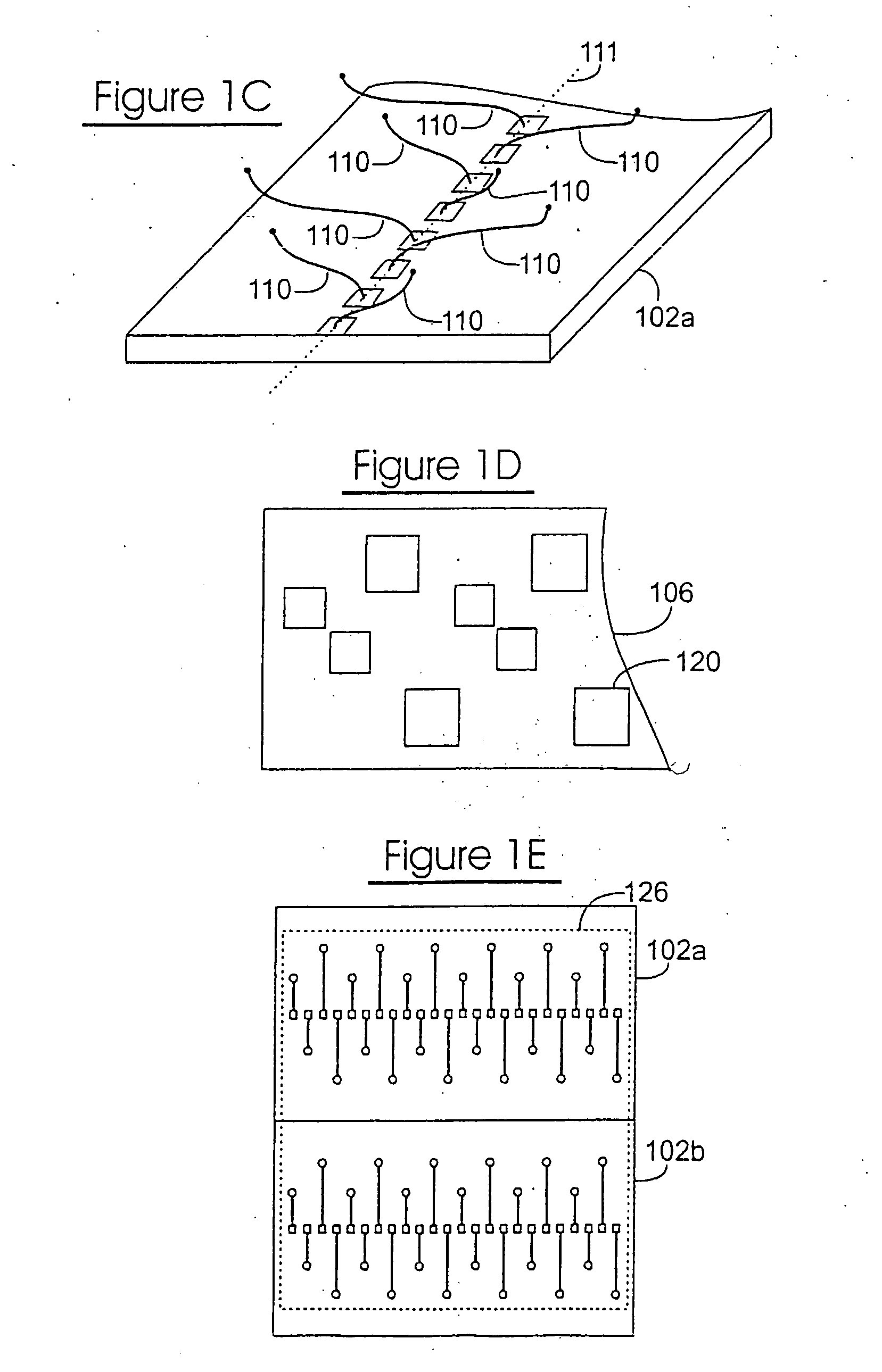
[0074] A plurality (four of many shown) of relatively small active electronic components 106a, 106b, 106c and 106d, such as application-specific integrated circuits (ASICs; referred to generally as element 106) are mounted to a relatively large interconnection substrate (base plate) 108 which is generally of the same size (i.e., diameter) as the WUT 102. For example, the interconnection substrate 108 and the WUT 102 are both eight or twelve inches in diameter. Together, the electronic components (ASICs) 106 and the interconnection substrate 108 constitute a “test substrate”.

[007...


PUM


Abstract

Techniques for performing wafer-level burn-in and test of semiconductor devices include a test substrate having active electronic components such as ASICs mounted to an interconnection substrate or incorporated therein, metallic spring contact elements effecting interconnections between the ASICs and a plurality of devices-under-test (DUTs) on a wafer-under-test (WUT), all disposed in a vacuum vessel so that the ASICs can be operated at temperatures independent from and significantly lower than the burn-in temperature of the DUTs. The spring contact elements may be mounted to either the DUTs or to the ASICs, and may fan out to relax tolerance constraints on aligning and interconnecting the ASICs and the DUTs. Physical alignment techniques are also described.

Description

CROSS-REFERENCE TO RELATED APPLICATIONS [0001] This patent application is a continuation-in-part of commonly-owned, copending U.S. patent application Ser. No. 08 / 452,255 (hereinafter “PARENT CASE”) filed 26 May 1995 and its counterpart PCT patent application number US95 / 14909 filed 13 Nov. 1995, both of which are continuations-in-part of commonly-owned, copending U.S. patent application Ser. No. 08 / 340,144 filed 15 Nov. 1994 and its counterpart PCT patent application number US94 / 13373 filed 16 Nov. 1994, both of which are continuations-in-part or commonly-owned, copending U.S. patent application Ser. No. 08 / 152,8712 filed 16 Nov. 1993 (now U.S. Pat. No. 5,476,211, 19 Dec. 1995), all of which are incorporated by reference herein. [0002] This patent application is also a continuation-in-part of the following commonly-owned, copending U.S. patent application Ser. Nos.: [0003] 08 / 526,246 filed 21 Sep. 1995 (PCT / US95 / 14843, 13 Nov. 1995); [0004] 08 / 533,584 filed 18 Oct. 1995 (PCT / US95 / 14...

Claims


Application Information

Patent Timeline
IPC IPC(8): G01R31/02G01R31/26
CPCG01R31/287G01R31/2874H01L2924/01079G01R31/318511H01L2924/01078G01R31/2886
Inventor KHANDROS, IGOR Y.PEDERSEN, DAVID V.
Owner FORMFACTOR INC
Why Eureka
Try Eureka