Defect detection system

a detection system and defect technology, applied in the field of defect detection, can solve the problems of system design, system optimization, single detector output becoming saturated, etc., and achieve the effect of facilitating the process of real-time defect classification and reducing cross-talk

Inactive Publication Date: 2005-01-27
VAEZ IRAVANI MEHDI +4
View PDF38 Cites 10 Cited by
  • Summary
  • Abstract
  • Description
  • Claims
  • Application Information

AI Technical Summary

Benefits of technology

[0009] One aspect of the invention is based on the observation that the collectors in the SP1TBI instruments preserve the azimuthal information of the scattered radiation by the surface inspected. Thus, by segmenting and directing the scattered radiation collected by the type of collectors used in the SP1TB1 instruments at different azimuthal positions to separate collection channels, the above-described difficulties are overcome so that an instrument may be constructed which is also optimized for the detection of patterned wafers. In this manner, a compact instrument can be achieved for measuring defects of patterned wafers. In addition to the ellipsoidal mirror used in the SP1TMI instruments, other azimuthally symmetric collectors may be used, such as a paraboloidal mirror used together with one or more lenses.
[0010] As in the SP1TBI system, the surface inspection system of one aspect of this invention collects radiation scattered from the surface by means of a collector that collects scattered radiation substantially symmetrically about a line normal to the surface. By directing to different channels the collected radiation scattered at different azimuthal angles about the line or another direction, these channels will carry information related to scattered radiation at corresponding relative azimuthal positions of the scattered radiation. Preferably, the channels are separated from each other by separators to reduce cross-talk. The collected scattered radiation carried by at least some of the channels may then be used for determining the presence and / or characteristics of anomalies in or on the surface. In addition, the multiple views of the same event can significantly facilitate the process of real time defect classification (RTDC).
[0011] In the above-described scheme, if only a portion of the collected radiation is directed to the different channels, while another portion of the collected radiation at different azimuthal angles are directed to a single detector for providing a single output as in the conventional SP1TBI scheme, the system can then be used for inspecting both unpatterned and patterned wafers. In other words, if the SP1TBI scheme is modified by diverting a portion of the collected radiation in the manner described above to different channels while preserving azimuthal information, a versatile tool results that can be optimized for the inspection of both unpatterned and patterned wafers. In this manner, semiconductor manufacturers no longer have to employ two different tools, each optimized for the detection of patterned or unpatterned wafers.

Problems solved by technology

While the SP1TBI system provides unsurpassed defect sensitivity on bare wafers or unpatterned wafers, this is not the case when it is used for inspecting wafers with patterns thereon such as wafers with memory arrays.
Thus, since pattern on the wafer will generate Fourier and / or other strong scattering signals, when these signals are collected and sent to the detector, the single detector output becomes saturated and unable to provide information useful for detecting defects on the wafer.
While inspection systems for detecting patterned wafers may be also used for inspecting unpatterned wafers, such systems are typically not optimized for such purposes.
Systems designed for the inspection of unpatterned or bare wafers, on the other hand, may have difficulties handling the diffraction or other scattering caused by the patterned structures on patterned wafers, for reasons such as those explained above.
The design of such spatial filters can be based on prior knowledge of the patterned structures and can be quite complex.
None of the above-described instruments is entirely satisfactory for the inspection of patterned wafers.
The CMP process, however, also creates many types of defects that can significantly impact the yield of an integrated circuit (IC) device if the defects are not properly controlled.
Among the CMP defects, the micro-scratch has a strong impact on IC yield.
One disadvantage of such instruments is the slow speed of their operation.

Method used


Image

  • Defect detection system
  • Defect detection system
  • Defect detection system

Examples


Embodiment Construction

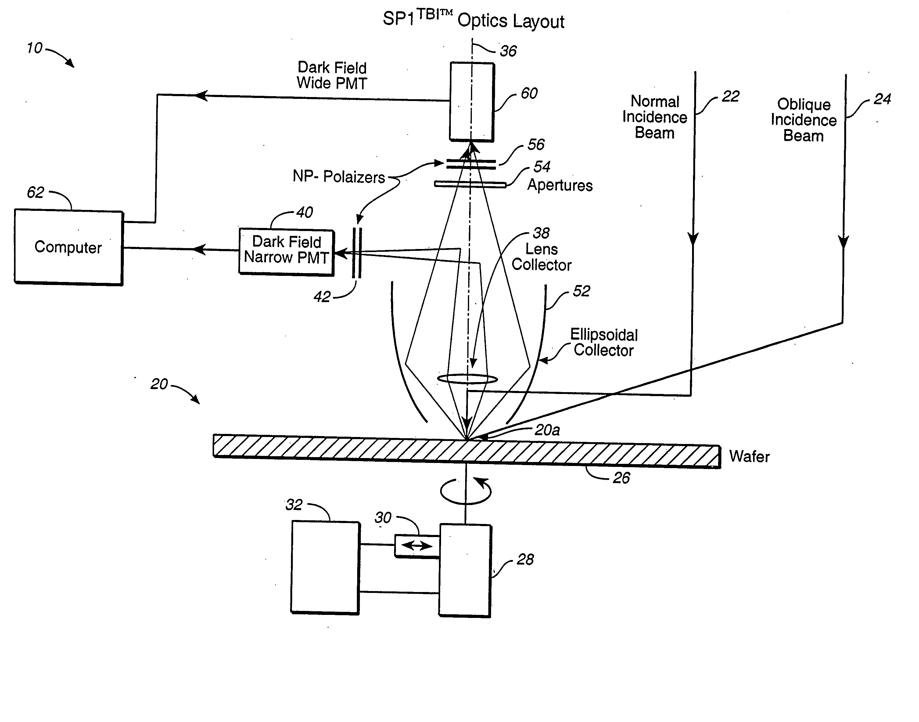
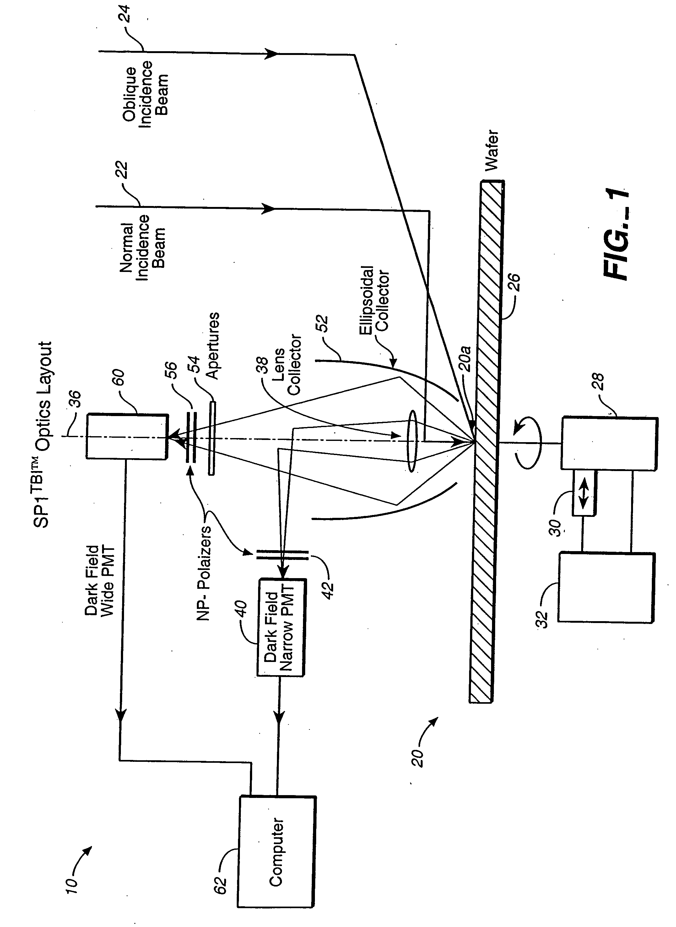
[0041]FIG. 1 is a schematic view of the SP1TBI system 10 available from KLA-Tencor Corporation of San Jose, Calif., the assignee of the present application. Aspects of the SP1TBI system 10 are described in U.S. patent application Ser. No. 08 / 770,491, filed Dec. 20, 1996 and U.S. Pat. No. 6,201,601, both of which are incorporated in their entireties by reference. To simplify the figure, some of the optical components of the system have been omitted, such as components directing the illumination beams to the wafer. The wafer 20 inspected is illuminated by a normal incidence beam 22 and / or an oblique incidence beam 24. Wafer 20 is supported on a chuck 26 which is rotated by means of a motor 28 and translated in a direction by gear 30 so that beams 22 and / or 24 illuminates an area or spot 20a which is caused to move and trace a spiral path on the surface of wafer 20 to inspect the surface of the wafer. Motor 28 and gear 30 are controlled by controller 32 in a manner known to those skill...


PUM

PropertyMeasurementUnit
elevational collection anglesaaaaaaaaaa
cell sizeaaaaaaaaaa
cell sizeaaaaaaaaaa

Abstract

Scattered radiation from a sample surface is collected by means of a collector that collects radiation substantially symmetrically about a line normal to the surface. The collected radiation is directed to channels at different azimuthal angles so- that information related to relative azimuthal positions of the collected scattered radiation about the line is preserved. The collected radiation is converted into respective signals representative of radiation scattered at different azimuthal angles about the line. The presence and / or characteristics of anomalies are determined from the signals. Alternatively, the radiation collected by the collector may be filtered by means of a spatial filter having an annular gap of an angle related to the angular separation of expected pattern scattering. Signals obtained from the narrow and wide collection channels may be compared to distinguish between micro-scratches and particles. Forward scattered radiation may be collected from other radiation and compared to distinguish between micro-scratches and particles. Intensity of scattering is measured when the surface is illuminated sequentially by S- and P-polarized radiation and compared to distinguish between micro-scratches and particles. Representative films may be measured using profilometers or scanning probe microscopes to determine their roughness and by the above-described instruments to determine haze in order to build a database. Surface roughness of unknown films may then be determined by measuring haze values and from the database.

Description

CROSS REFERENCE TO RELATED APPLICATION [0001] This application is related to U.S. patent application Ser. No. 08 / 770,491, filed Dec. 20, 1996, U.S. Pat. No. 6,201,601, issued Mar. 13, 2001 and the application being filed concurrently herewith. The related applications and the issued patent are incorporated herein by reference in their entireties.BACKGROUND OF THE INVENTION [0002] This invention relates in general to defect detection, and, in particular, to an improved system for detecting anomalies on surfaces, such as particles and surface-originated defects such as crystal-originated particles (“COPs”), surface roughness and micro-scratches. [0003] The SP1TBI™ detection system available from KLA-Tencor Corporation of San Jose, Calif., the Assignee of the present application, is particularly useful for detecting defects on unpatterned semiconductor wafers. While the SP1TBI system provides unsurpassed defect sensitivity on bare wafers or unpatterned wafers, this is not the case when...

Claims


Application Information

Patent Timeline
Patent Type & Authority Applications(United States)
IPC IPC(8): G01N21/21G01N21/95
CPCG01N21/21G01N21/956G01N21/9501
Inventor VAEZ-IRAVANI, MEHDIRZEPIELA, JEFFREY ALANTREADWELL, CARLZENG, ANDREWFIORDALICE, ROBERT
Owner VAEZ IRAVANI MEHDI
Why Eureka
Try Eureka