
Strained semiconductor by wafer bonding with misorientation

a technology of misorientation and semiconductor, applied in the field of semiconductor devices formed with strained semiconductor films, can solve the problems of large mismatch between cell structures, high cost and complex process of uhvcvd process, etc., and achieve the effect of simple and low cost wafer bonding technique and enhanced carrier mobility

Inactive Publication Date: 2005-02-03
MICRON TECH INC
View PDF0 Cites 66 Cited by
  • Summary
  • Abstract
  • Description
  • Claims
  • Application Information

AI Technical Summary

Benefits of technology

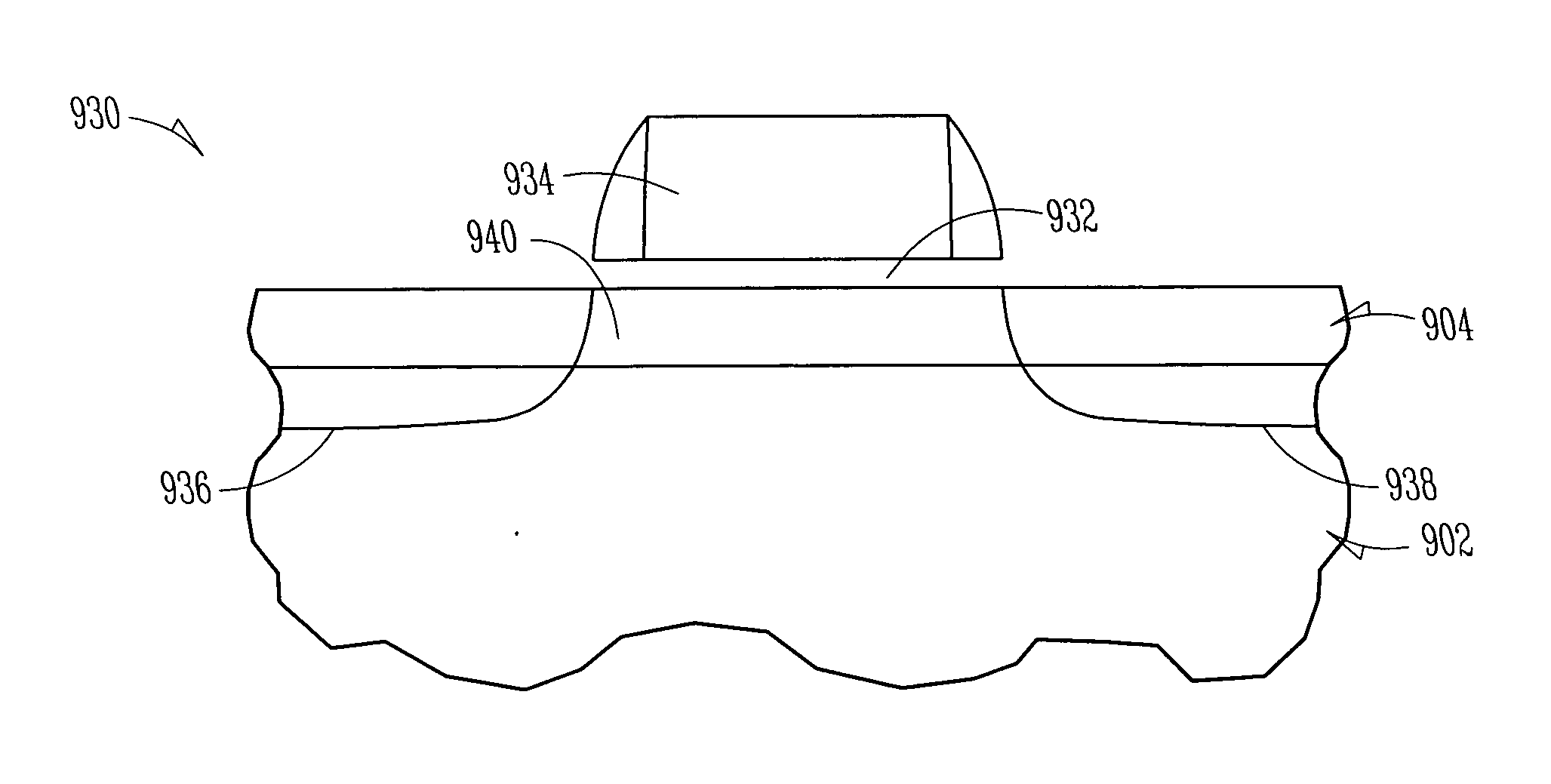
The patent describes a method for creating strained semiconductor films, which can enhance carrier mobility and improve device performance. The method involves bonding a thin semiconductor layer to a substrate with a desired tilt / twist misorientation to create a desired strain in the layer. The bonding process involves creating strong bonding regions between the layer and the substrate, separated by a weak bonding region. The membrane is then pinned in the strong bonding regions, resulting in a desired strain in the membrane. The strain can be created by a predetermined misorientation or a predetermined tilt angle between the membrane and the substrate. The resulting strained semiconductor structure can be used in various electronic devices, such as solar cells or semiconductor lasers.

Problems solved by technology

There is a large mismatch in the cell structure between the Si and SiGe layers.
The UHVCVD process is a costly and complex process.

Method used


Image

  • Strained semiconductor by wafer bonding with misorientation
  • Strained semiconductor by wafer bonding with misorientation
  • Strained semiconductor by wafer bonding with misorientation

Examples


Embodiment Construction

The following detailed description refers to the accompanying drawings which show, by way of illustration, specific aspects and embodiments in which the present invention may be practiced. The various embodiments of the present invention are not necessarily mutually exclusive as aspects of two or more embodiments can be combined to form other embodiments. Other embodiments may be utilized and structural, logical, and electrical changes may be made without departing from the scope of the present invention. In the following description, the terms wafer and substrate are interchangeably used to refer generally to any structure on which integrated circuits are formed, and also to such structures during various stages of integrated circuit fabrication. Both terms include doped and undoped semiconductors, epitaxial layers of a semiconductor on a supporting semiconductor or insulating material, combinations of such layers, as well as other such structures that are known in the art. The te...


PUM


Abstract

One aspect of the present invention relates to a method for forming a strained semiconductor structure. In various embodiments, at least two strong bonding regions are defined for a desired bond between a crystalline semiconductor membrane and a crystalline semiconductor substrate. The two strong bonding regions are separated by a weak bonding region. The membrane is bonded to the substrate at a predetermined misorientation. The membrane is pinned to the substrate in the strong bonding regions. The predetermined misorientation provides the membrane in the weak bonding region with a desired strain. In various embodiments, the membrane is bonded to the substrate at a predetermined twist angle to biaxially strain the membrane in the weak bonding region. In various embodiments, the membrane is bonded to the substrate at a predetermined tilt angle to uniaxially strain the membrane in the weak bonding region. Other aspects are provided herein.

Description

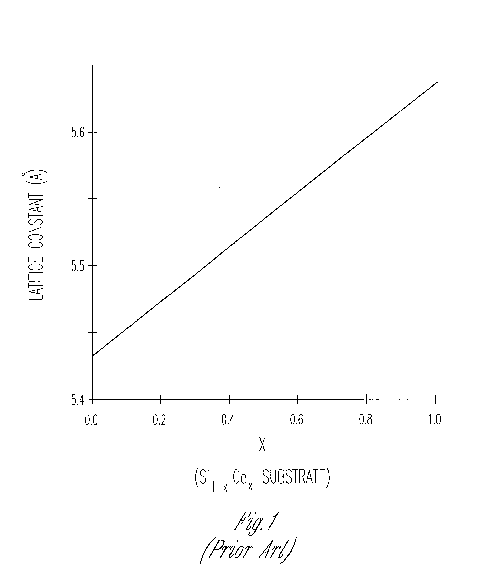
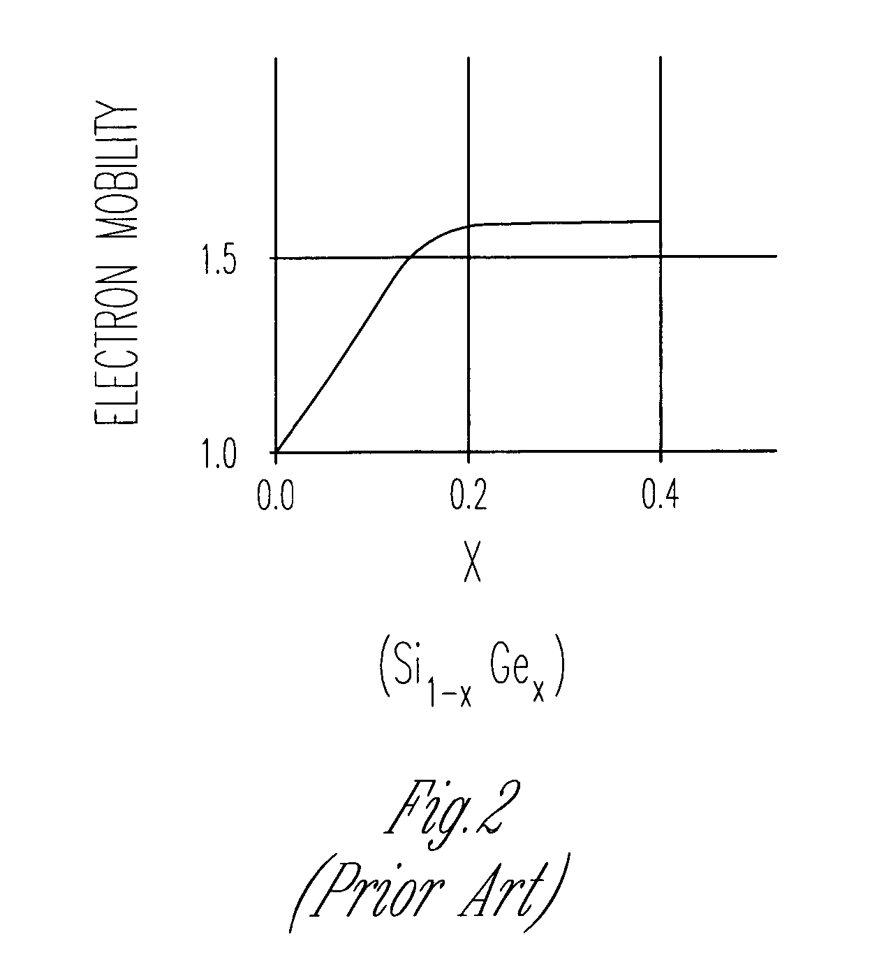
TECHNICAL FIELD This disclosure relates generally to semiconductor devices, and more particularly, to devices formed with strained semiconductor films. BACKGROUND The semiconductor industry continues to strive for improvements in the speed and performance of semiconductor devices. Strained silicon technology enhances carrier mobility in both n-channel and p-channel devices, and thus improves device speed and performance. One technique for producing strained silicon involves growing silicon on relaxed silicon germanium (Si / SiGe) structures. There is a large mismatch in the cell structure between the Si and SiGe layers. This mismatch causes a pseudomorphic layer of Si on relaxed SiGe to be under a biaxial tensile strain that modifies the band structure and enhances carrier transport in the Si layer. In an electron inversion layer, the subband splitting is larger in strained Si because of the strain-induced band splitting in addition to that provided by quantum confinement. For exam...

Claims


Application Information

Patent Timeline
Patent Type & Authority Applications(United States)
IPC IPC(8): H01L21/18H01L29/04
CPCH01L21/187H01L21/26506H01L21/76251H01L21/823412Y10S438/938H01L27/10873H01L29/045H01L29/1054H01L29/7842H01L21/84H10B12/05
Inventor FORBES, LEONARD
Owner MICRON TECH INC
Learn More