
Electrostatic discharge protection devices having transistors with textured surfaces

a technology of textured surfaces and protection devices, which is applied in the direction of semiconductor devices, semiconductor/solid-state device details, electrical apparatus, etc., can solve the problems of reducing sb>1/b> and sb>2/b>, preventing circuits from being damaged, and reducing the sb>1/b> and sb>2/b> to be adequate for esd current to discharge, etc., to increase the surface area o

Inactive Publication Date: 2005-02-03
MICRON TECH INC
View PDF45 Cites 1 Cited by
  • Summary
  • Abstract
  • Description
  • Claims
  • Application Information

AI Technical Summary

Benefits of technology

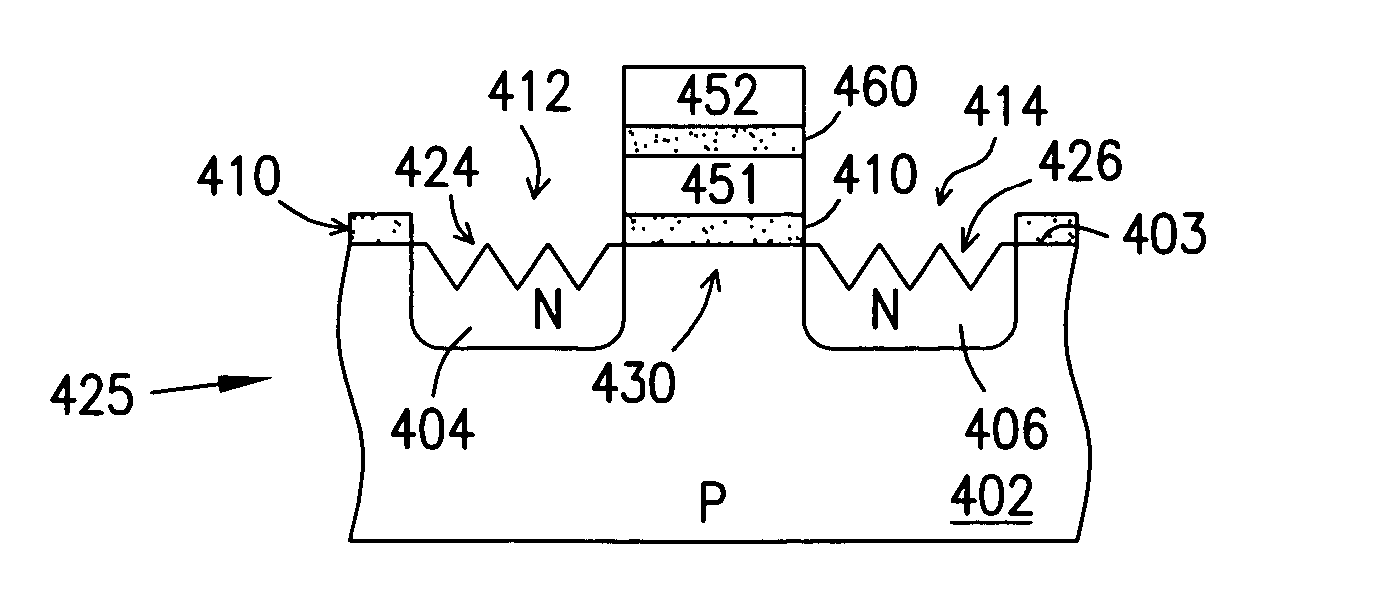
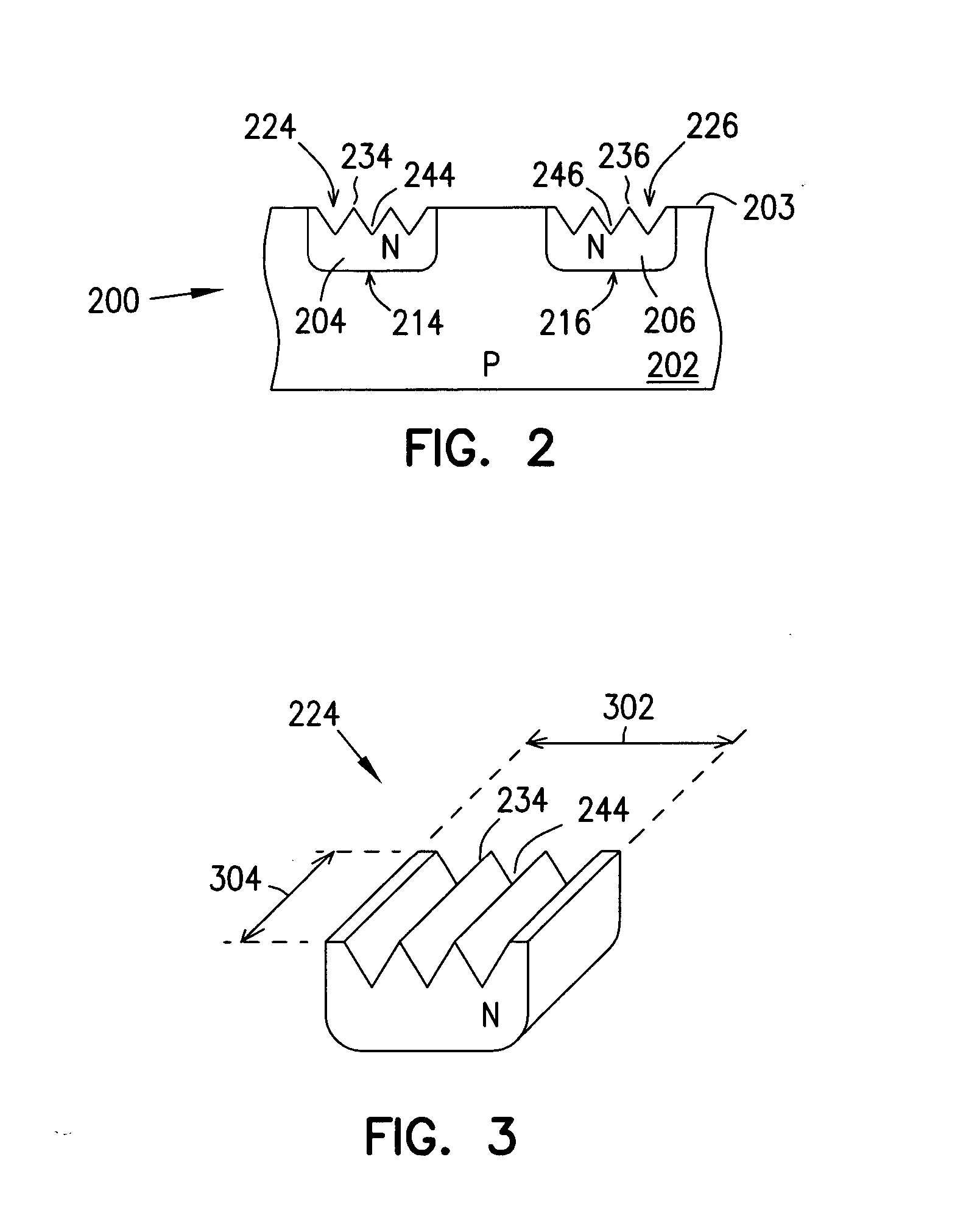
The present invention provides transistors and diodes with reduced dimensions to save space while maintaining adequate surface areas for sufficient protection. The reduced size allows for smaller bonding pads, making the circuit size smaller or allowing for more components without increasing the circuit size. The transistors and diodes have textured surfaces that increase their surface area, leading to increased current passing through the contact surfaces and decreased contact resistance, allowing more heat to dissipate. The technical effects of the invention include reduced space requirements, increased protection, and improved heat dissipation.

Problems solved by technology

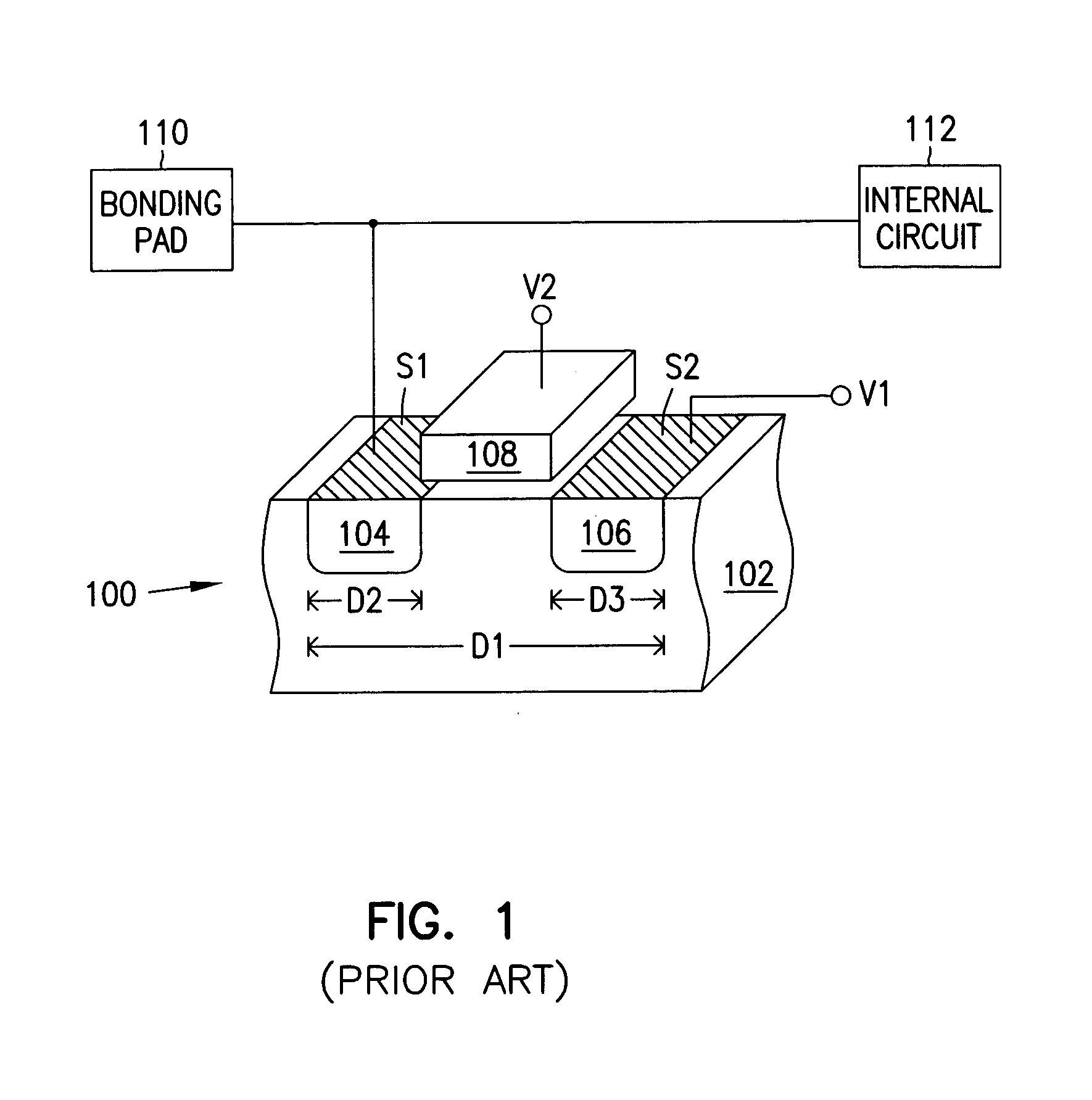
Without a protection device, a large ESD current and the heat created by the ESD event could flow from the bonding pad to internal elements of the circuit and potentially damage these internal elements.
When transistor 100 serves as an ESD protection device, the reduced S1 and S2 may not be adequate for the ESD current to discharge.
This may damage transistor 100 itself or cause it to protect the circuit inadequately.

Method used


Image

  • Electrostatic discharge protection devices having transistors with textured surfaces
  • Electrostatic discharge protection devices having transistors with textured surfaces
  • Electrostatic discharge protection devices having transistors with textured surfaces

Examples


Embodiment Construction

[0034] The following description and the drawings illustrate specific embodiments of the invention sufficiently to enable those skilled in the art to practice it. Other embodiments may incorporate structural, logical, electrical, process, and other changes. In the drawings, like numerals describe substantially similar components throughout the several views. Examples merely typify possible variations. Portions and features of some embodiments may be included in or substituted for those of others. The scope of the invention encompasses the full ambit of the claims and all available equivalents.

[0035]FIG. 2 is a cross-section of a bipolar transistor having a textured surface according to an embodiment of the invention. Transistor 200 includes a substrate 202 and doped regions 204 and 206 formed in the substrate. Substrate 202, doped regions 204 and 206 include semiconductor material, for example, silicon. Substrate 202 is doped with one kind of dopant (or impurity) to make it a first...


PUM


Abstract

An electrostatic discharge (ESD) protection device connects to a bonding pad and an internal circuit for protecting the internal circuit during an ESD event. The ESD protection device includes a transistor connected between the bonding pad and a supply node. The transistor includes a first doped region having a textured surface connected to the bonding pad, and a second doped region having a textured surface connected to the supply node.

Description

RELATED APPLICATIONS [0001] This application is a divisional of U.S. application Ser. No. 10 / 226,678 filed on Aug. 23, 2002 which is incorporated herein by reference.FIELD [0002] The present invention relates generally to semiconductor devices, and in particular to electrostatic discharge protection devices. BACKGROUND [0003] Semiconductor devices such as transistors are widely used as switches in electrical circuits to control the flow of current. Many circuits use transistors to protect them from an electrostatic discharge (ESD) event. An ESD event occurs when an external voltage much higher than the normal operating voltage of the circuit appears at bonding pads or external pins of the circuit. Human or other elements could cause the ESD event. Without a protection device, a large ESD current and the heat created by the ESD event could flow from the bonding pad to internal elements of the circuit and potentially damage these internal elements. [0004]FIG. 1 is a cross-section of a...

Claims


Application Information

Patent Timeline
Patent Type & Authority Applications(United States)
IPC IPC(8): H01L21/285H01L21/336H01L21/768H01L27/02H01L29/06
CPCH01L21/28512H01L21/76895H01L27/0251H01L29/0657H01L2924/0002H01L29/66636H01L2924/00H01L29/78H01L29/0847
Inventor FARNWORTH, WARREN M.BISSEY, LUCIEN J.
Owner MICRON TECH INC
Learn More