Topless semiconductor package

Active Publication Date: 2005-02-10
INFINEON TECH AMERICAS
View PDF9 Cites 18 Cited by
  • Summary
  • Abstract
  • Description
  • Claims
  • Application Information

AI Technical Summary

Benefits of technology

[0012] An objective of the present invention is a semiconductor

Problems solved by technology

While heat dissipation is improved in the packages of the latter type, the position of the exposed portion of the die pad (the bottom surface of the molded housing) is less than ideal for heat dissipation by convection.
Moreover, exposing the die pad at the bottom of the molded housing restricts the size of the heat spreader or the heatsink that may be used in that a) the lateral

Method used


Image

  • Topless semiconductor package
  • Topless semiconductor package
  • Topless semiconductor package

Examples


Embodiment Construction

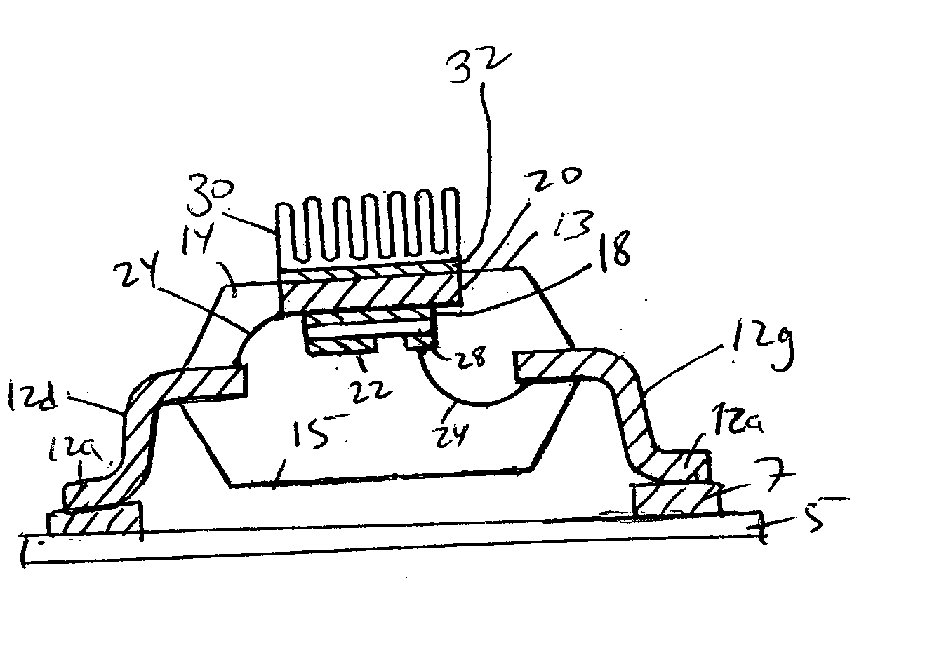
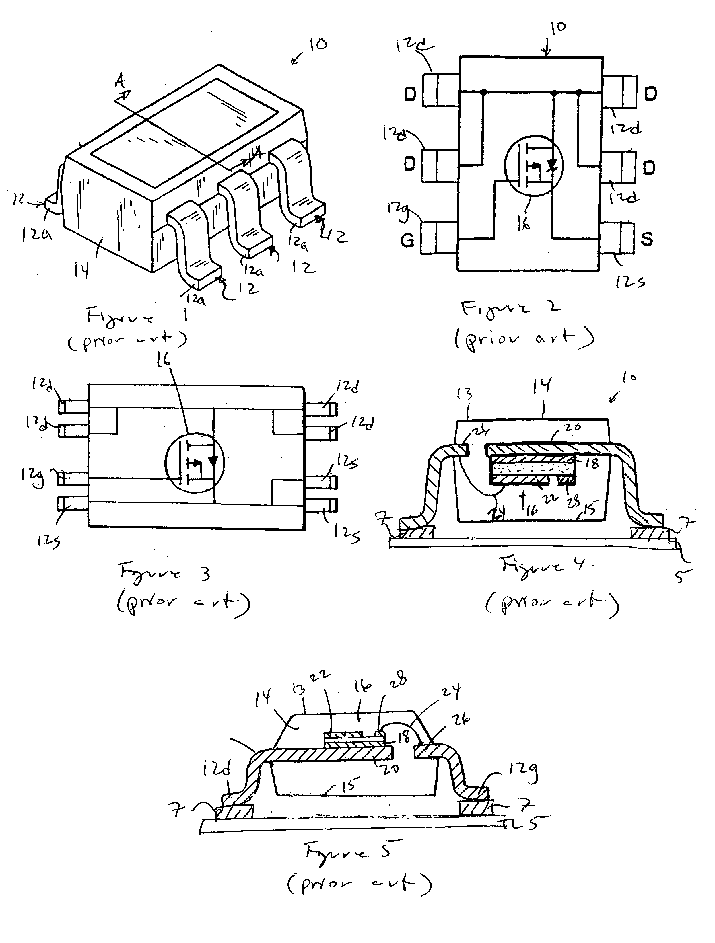
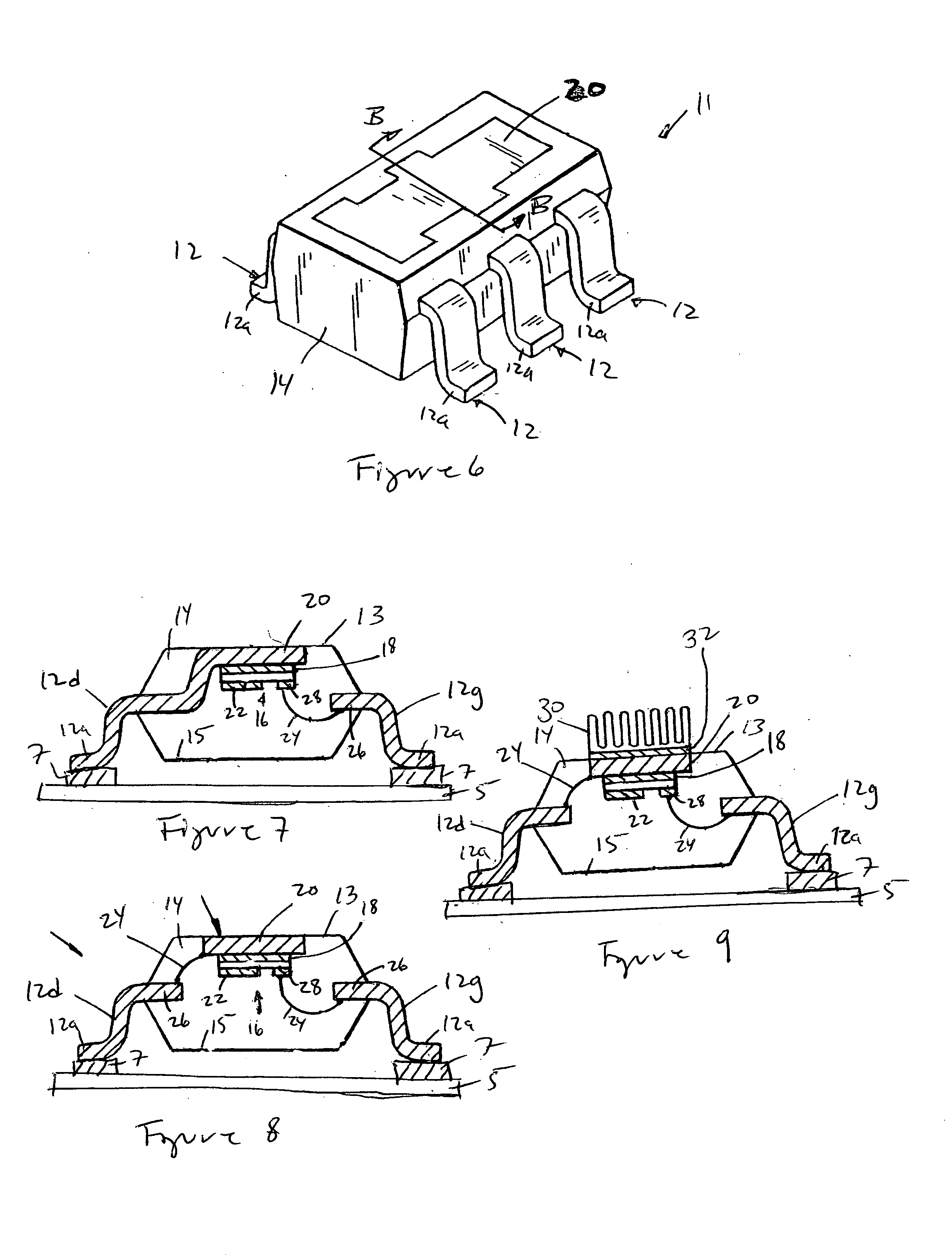
[0037] Referring now to FIG. 6, in which like elements are identified with like numerals, a semiconductor package 11 according to the present invention includes die pad 20 which is exposed through molded housing 14. Specifically, according to the present invention, die pad 20 is exposed through top surface 13 of molded housing 14, i.e., the surface which is farthest from substrate 15 when package 11 is mounted.

[0038] Referring to FIG. 7, in a semiconductor package 20 according to the first embodiment of the present invention, a semiconductor device, such as power MOSFET 16, is mounted on the bottom surface of die pad 20, and the opposing top surface of die pad 20 is exposed through top surface 13 of molded housing 14. Thus, for example, in the preferred embodiment of the present invention in which power MOSFET 16 is the semiconductor device, drain electrode 18 of power MOSFET 16 is electrically and mechanically connected by a conductive adhesive such as solder or conductive epoxy t...


PUM


Abstract

A semiconductor package which includes a die pad that is exposed through the top surface of its molded housing.

Description

RELATED APPLICATION [0001] This application is based on and claims benefit of U.S. Provisional Application No. 60 / 493,065, filed on Aug. 5, 2003, entitled Topless Semiconductor Package, to which a claim of priority is hereby made and the disclosure of which is incorporated by reference.BACKGROUND OF THE INVENTION [0002]FIG. 1 shows a perspective external view of a semiconductor package 10 according to the prior art. Semiconductor package 10 includes leads 12 which extend outwardly from molded housing 14 of semiconductor package 10. Semiconductor package 10 is an example of a standard small outline surface mounted package which is adapted for surface mounting onto a substrate 5 (FIG. 4), such as a circuit board. Specifically, leads 12 have been adapted to include terminal ends 12a which can be received by conductive pads 7 (FIG. 4) on a substrate 5 (FIG. 4). Leads 12 thus serve to support a package on a substrate. [0003] Leads 12 further serve as electrical connectors for the semicon...

Claims


Application Information

Patent Timeline
IPC IPC(8): H01L23/31H01L23/495
CPCH01L23/3107H01L23/49562H01L2924/1305H01L2924/014H01L2924/01033H01L24/48H01L2924/19107H01L2924/1532H01L2924/14H01L2924/13091H01L2924/13055H01L2924/01082H01L2924/01079H01L2924/01047H01L24/45H01L24/49H01L2224/32245H01L2224/45144H01L2224/48091H01L2224/48247H01L2224/49H01L2224/73265H01L2924/01004H01L2924/01005H01L2924/01006H01L2924/01029H01L2924/00014H01L2924/00H01L2924/181H01L2924/00012
Inventor AMBRUS, JOHN
Owner INFINEON TECH AMERICAS
Why Eureka
Try Eureka