Optical recording/reproducing medium-use substrate, production method for optical recording/reproducing medium reproducing stamper and optical recording/reproducing medium producing stamper
a technology substrate, which is applied in the field of optical recording/reproducing medium substrate, can solve the problems of inability to easily form groove widths, inability to directly apply conventional manufacturing methods to optical disks, and inability to achieve satisfactory recording and reproducing characteristics, and achieve high accuracy. the effect of high yield
- Summary
- Abstract
- Description
- Claims
- Application Information
AI Technical Summary
Benefits of technology
Problems solved by technology
Method used
Image
Examples
##ventive example 1
INVENTIVE EXAMPLE 1
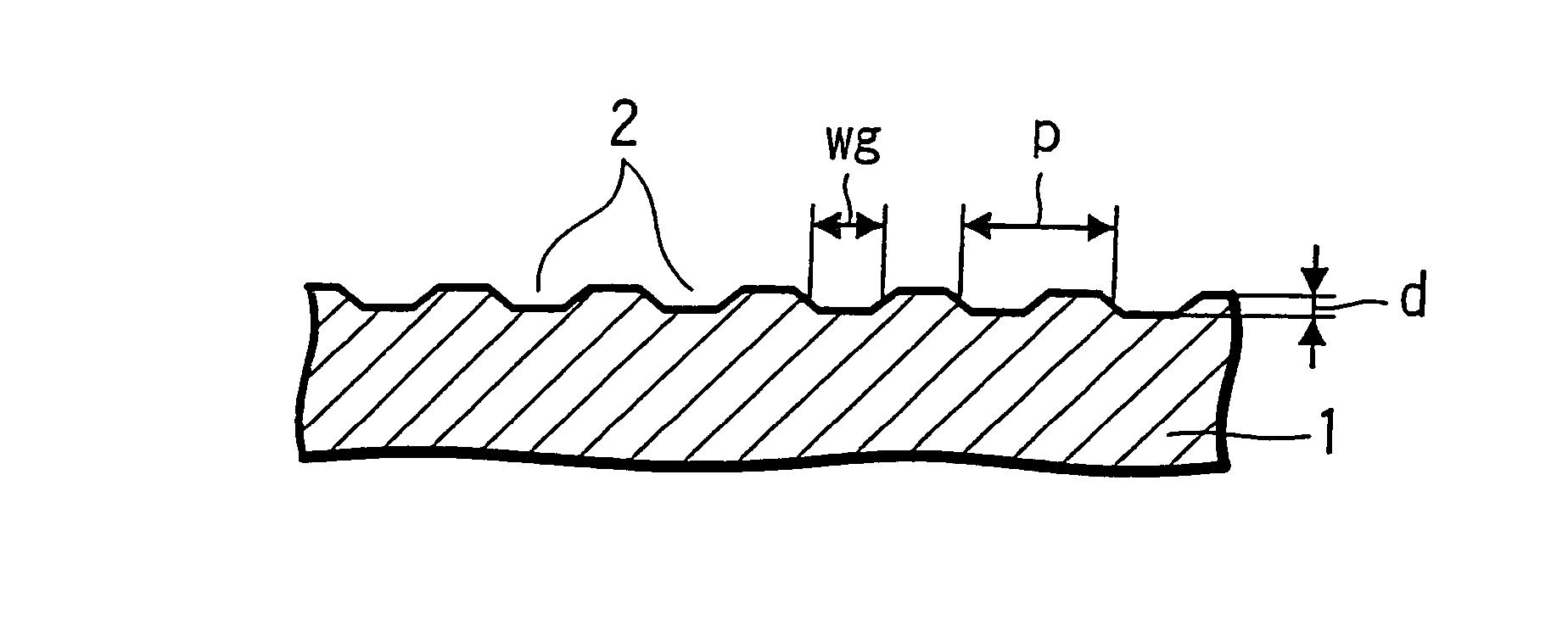
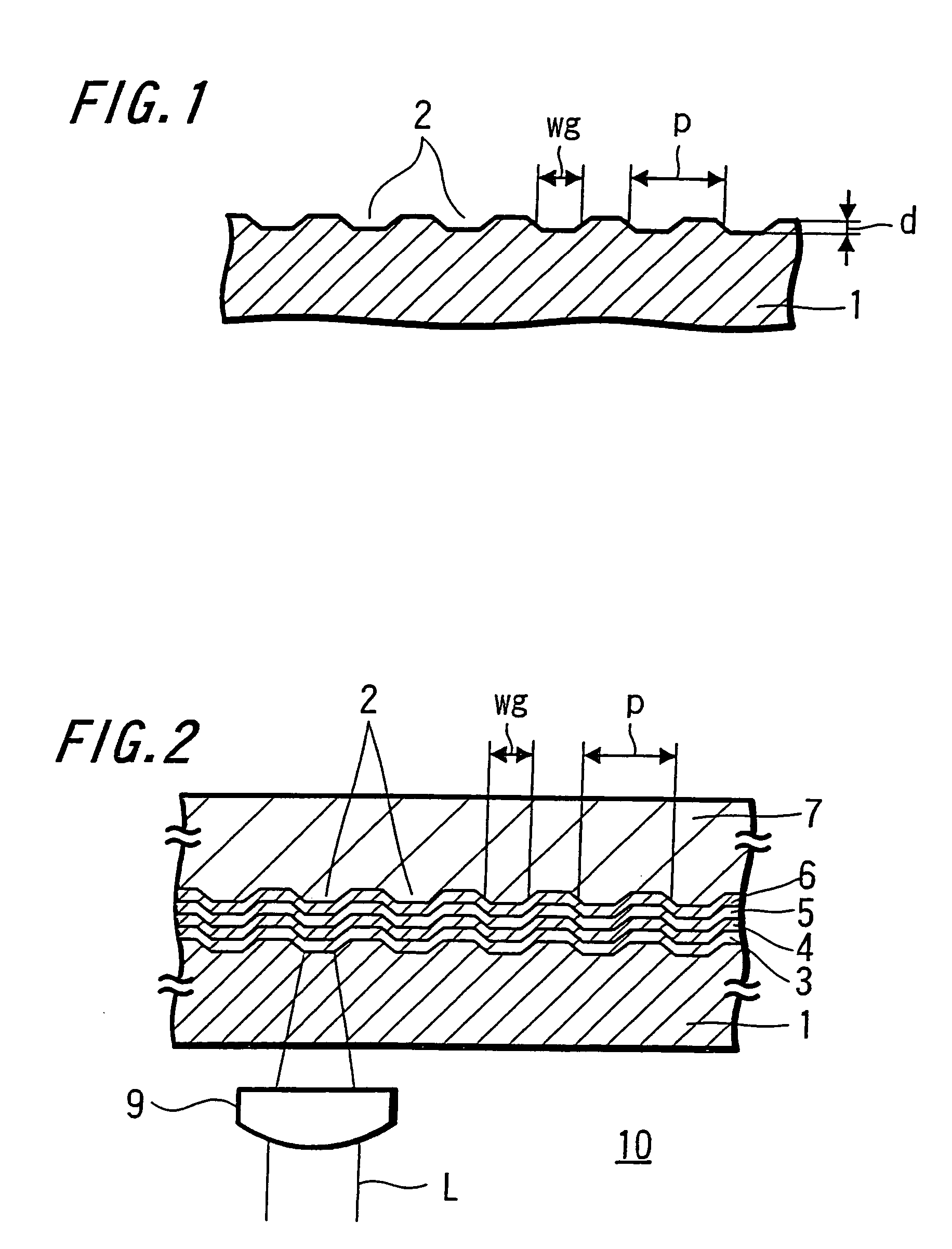
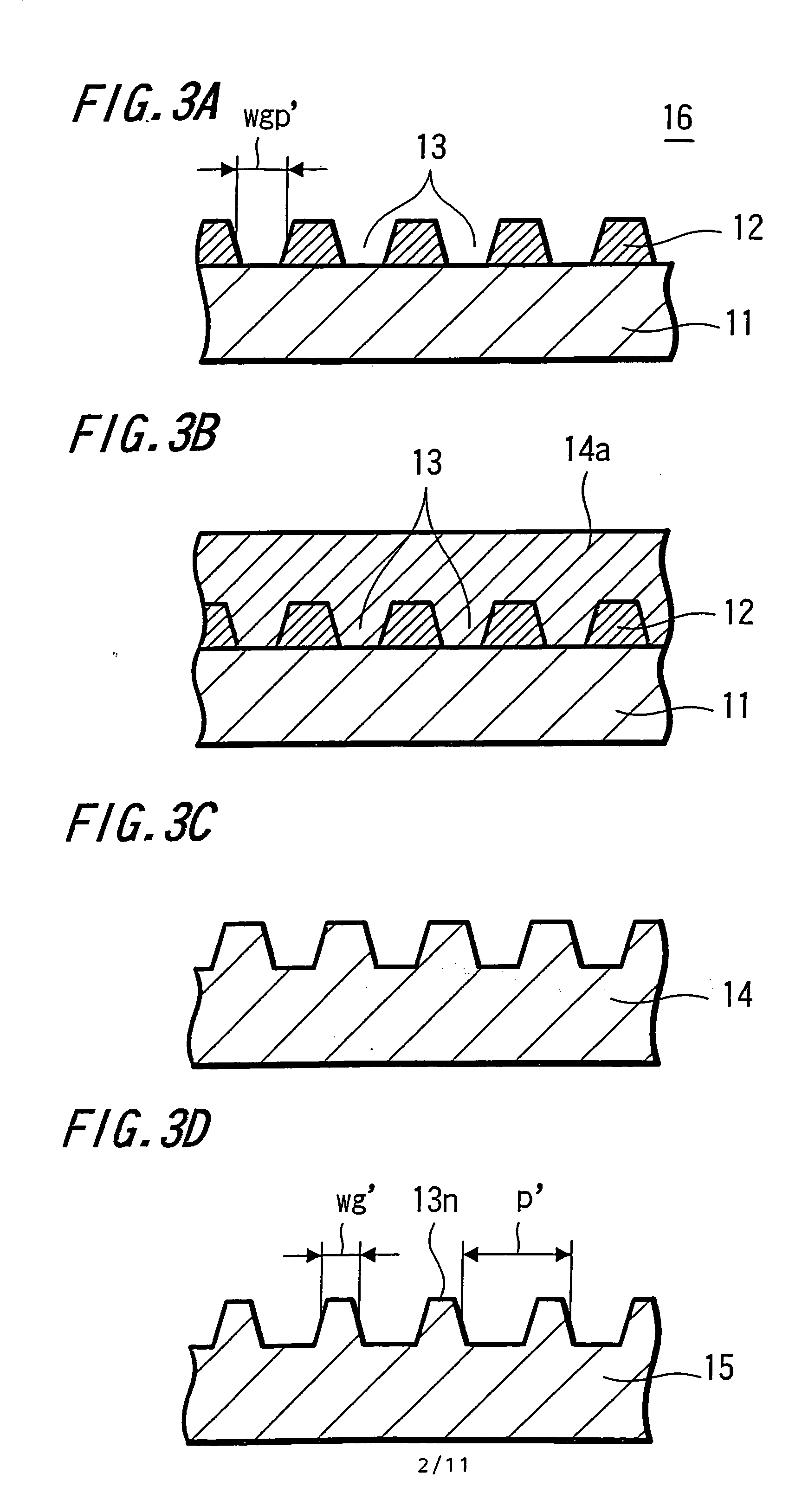
[0116] In the conditions in which a Kr laser (wavelength λ=351 nm) was used as a light source, laser power was controlled so as to fall within a range of from 76% to 100% where 0.6 mJ / m was maximum (100%) and a feed pitch was selected to be 0.350 μm, i.e., a track pitch was selected to be 0.35 μm (350 nm), an optical recording and reproducing medium manufacturing master was manufactured by effecting optical recording on the photoresist. The depth of the groove pattern was set to 15 nm by adjusting the film thickness of the photoresist. A stamper that has been transferred and molded from that master was set to a stamper A. A stamper of which groove width has been microminiaturized by further etching the stamper A under the above-mentioned conditions was set to a stamper AE.
##ventive example 2
INVENTIVE EXAMPLE 2
[0117] In the conditions in which a Kr laser was used as a light source, laser power was controlled so as to fall within a range of from 77% to 100% where 0.25 mJ / m was maximum (100%) and a feed pitch was selected to be 0.300 μm, i.e., a track pitch was selected to be 0.30 μm (300 nm), an optical recording and reproducing medium manufacturing master was manufactured by effecting optical recording on the photoresist. The depth of the groove pattern was set to 20 nm by adjusting the film thickness of the photoresist. A stamper that has been transferred and molded from that master was set to a stamper B. A stamper of which groove width has been microminiaturized by further etching the stamper B under the above-mentioned conditions was set to a stamper BE.
##ventive example 3
INVENTIVE EXAMPLE 3
[0118] In the conditions in which a quartic higher harmonic wave (wavelength λ=266 nm) of a YAG laser was used as a light source, laser power was controlled so as to fall within a range of from 75% to 100% where 0.15 mJ / m was maximum (100%) and a feed pitch was selected to be 0.250 μm, i.e., a track pitch was selected to be 0.25 μm (250 nm), an optical recording and reproducing medium manufacturing master was manufactured by effecting optical recording on the photoresist. The depth of the groove pattern was set to 25 nm by adjusting the film thickness of the photoresist. A stamper that has been transferred and molded from that master was set to a stamper C. A stamper of which groove width has been microminiaturized by further etching the stamper C under the above-mentioned conditions was set to a stamper CE.
PUM
 Abstract
Description
Claims
Application Information


