Photomask, method for fabricating a pattern and method for manufacturing a semiconductor device

a technology of semiconductor devices and patterns, applied in the field of photolithographic technology, can solve the problems of difficult to reduce a systematic step generated on the surface of an interlayer dielectric film deposited on the wiring layer, difficult for cmp technology to adjust a focus position, and the inability to delineate the proper photoresist pattern

Inactive Publication Date: 2005-02-10
KK TOSHIBA
View PDF2 Cites 12 Cited by
  • Summary
  • Abstract
  • Description
  • Claims
  • Application Information

AI Technical Summary

Problems solved by technology

However, it is generally difficult to reduce a systematic step generated on a surface of an interlayer dielectric film deposited on a wiring layer, at a boundary between a dense wiring region and a sparse wiring or an isolated wiring region.
It is difficult for the CMP technology to adjust a focus position on both surfaces of the interlayer dielectric films on the dense and sparse wiring regions having the systematic step generated therebetween.
Consequently, a problem occurs such that a defocus is generated in one of the surfaces of the interlayer dielectric films and a proper photoresist pattern can not be delineated.
However, in some cases, the proper dummy pattern cannot be easily arranged in a sparse wiring region.
Therefore, it is difficult to achieve a sufficient planarization on a surface of an interlayer dielectric film for focusing.
Accordingly, even if the CMP technology is applied by arranging the dummy pattern in the sparse wiring region, generation of the systematic step may not be completely suppressed.
Hence, it is difficult to achieve sufficient planarization on a surface of an interlayer dielectric film for a proper depth of focus.
Thus, since the depth of focus of the aligner is insufficient for the systematic step, performance for delineating a pattern and a production yield of the semiconductor device are extremely decreased due to the generation of defects such as a failure of transferring a pattern with a desired dimension, deterioration of dimensional fidelity of the circuit pattern as short or open wiring fault and a collapse or scattering of a resist pattern.

Method used


Image

  • Photomask, method for fabricating a pattern and method for manufacturing a semiconductor device
  • Photomask, method for fabricating a pattern and method for manufacturing a semiconductor device
  • Photomask, method for fabricating a pattern and method for manufacturing a semiconductor device

Examples


Embodiment Construction

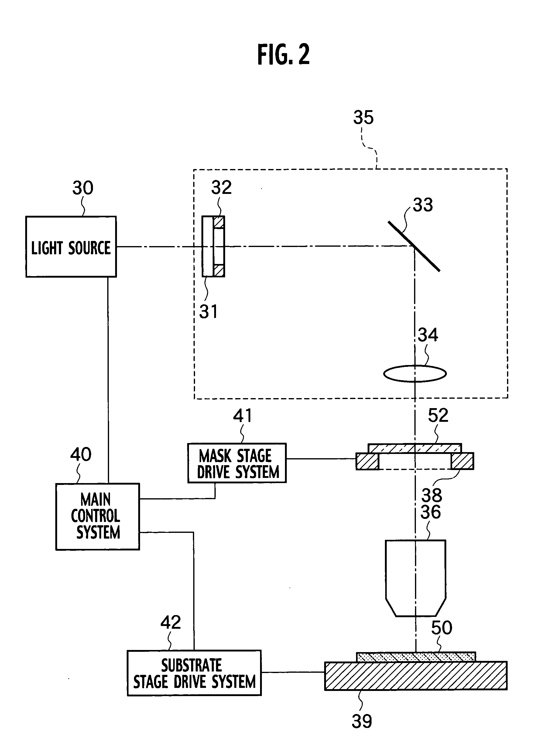
An embodiment of the present invention will be described with reference to the accompanying drawings. It is to be noted that the same or similar reference numerals are applied to the same or similar parts and elements throughout the drawings, and the description of the same or similar parts and elements will be omitted or simplified.

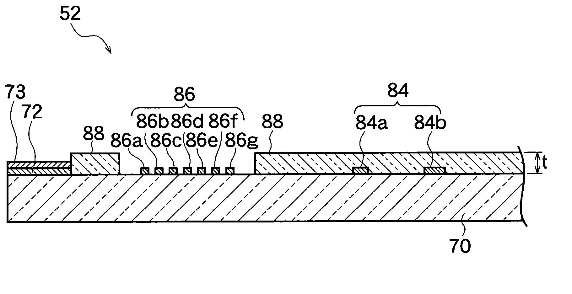
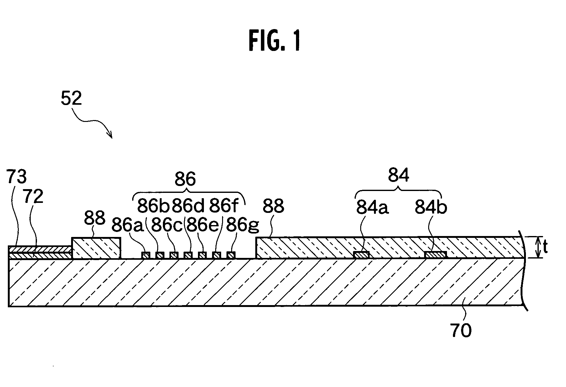
A photomask 52 according to an embodiment of the present invention, as shown in FIG. 1, includes a transparent substrate 70, a first mask pattern 84, a second mask pattern 86, and a transparent film 88. The first and second mask patterns 84, 86 are disposed on the transparent substrate 70, and the transparent film 88 having an actual film thickness of t, is located in a pattern region including the mask pattern 84 disposed therein. As the first mask pattern 84, first mask portions 84a, 84b are shown in the sectional view of FIG. 1, and as a second mask pattern 86, second mask portions 86a to 86g are shown in the cross-sectional view of FIG. 1. In addi...


PUM

PropertyMeasurementUnit
transmittanceaaaaaaaaaa
wavelengthaaaaaaaaaa
transparentaaaaaaaaaa

Abstract

A photomask includes a transparent substrate; a first mask pattern disposed on a first region of the transparent substrate; a second mask pattern disposed on a second region different from the first region of the transparent substrate; and a transparent film provided on the first mask pattern, having an optical thickness configured to make a focal position of the first mask pattern deeper than a focal position of the second mask pattern.

Description

CROSS REFERENCE TO RELATED APPLICATIONS This application is based upon and claims the benefit of priority from prior Japanese Patent Application P2003-289008 filed on Aug. 7, 2003; the entire contents of which are incorporated by reference herein. BACKGROUND OF THE INVENTION 1. Field of the Invention The present invention relates to photolithographic technology, and particularly relates to a photomask, a method for fabricating a pattern using the photomask, and a method for manufacturing a semiconductor device. 2. Description of the Related Art When forming a circuit pattern of a semiconductor device, a photosensitive material such as a photoresist is coated on a working film on a semiconductor substrate, which is then exposed using a reduction projection aligner and developed. When an aligner having a refraction optical system is used, a light emitted from a light source, passing through an illumination optical system and a projection optical system, and demagnifies and projec...

Claims


Application Information

Patent Timeline
Patent Type & Authority Applications(United States)
IPC IPC(8): G03C5/00G03F1/54G03F1/56G03F7/16G03F7/20G03F9/00G03G16/00H01L21/00H01L21/027
CPCG03F1/144G03F1/70
Inventor ITO, HITOSHI
Owner KK TOSHIBA
Why Eureka
Try Eureka