Embedded DRAM cache

a memory structure and cache technology, applied in the field of cache memory structures for processor based systems, can solve the problems of reducing increasing the number of cycles it takes to transfer data, and increasing the latency or number of cycles, so as to reduce the average memory latency, increase system bandwidth and overall performance, and reduce the effect of average memory latency

Inactive Publication Date: 2005-02-10
JEDDELOH JOSEPH M
View PDF15 Cites 4 Cited by
  • Summary
  • Abstract
  • Description
  • Claims
  • Application Information

AI Technical Summary

Benefits of technology

[0014] The present invention provides a third level of high speed cache memory (L3 cache) for a processor based system that is closer to the system processor with respect to the system memory, which reduces average memory latency and thus, increases system bandwidth and overall performance.
[0016] The present invention further provides an L3 cache for a processor based system that allows several requesting devices of the system to simultaneously access the contents of the L3 cache.
[0017] The above and other features and advantages are achieved by a large L3 cache that is integrated within the system chipset. The L3 cache is comprised of multiple embedded memory cache arrays. Each array is accessible independently of each other, providing parallel access to the L3 cache. By placing the L3 cache within the chipset, it is closer to the system processor with respect to the system memory. By using independent arrays, the L3 cache can handle numerous simultaneous requests. This reduces average memory latency and thus, increases system bandwidth and overall performance. By using embedded memory, the L3 cache can be implemented on the chipset and be much larger than the L1 and L2 caches without substantially increasing the size of the chipset and system.

Problems solved by technology

However, each level typically increases the latency or number of cycles it takes to transfer the data to the processor.
Increased latency reduces the system bandwidth and overall performance.

Method used


Image

  • Embedded DRAM cache
  • Embedded DRAM cache
  • Embedded DRAM cache

Examples


Embodiment Construction

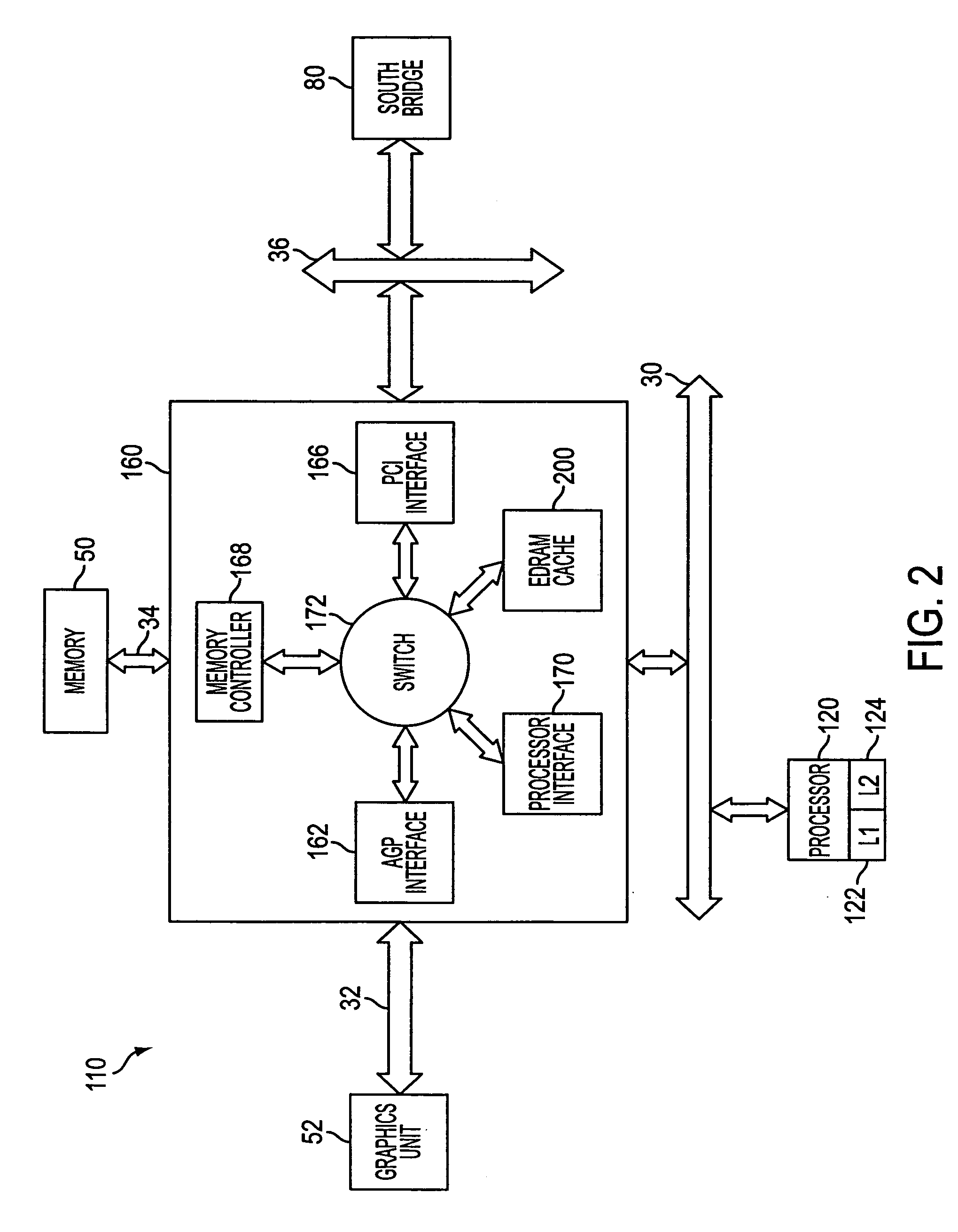
[0022]FIG. 2 illustrates a portion of a processor based system 110 having an eDRAM L3 cache 200 integrated on the system chipset constructed in accordance with an exemplary embodiment of the present invention. The system 110 includes a south bridge 80 and a north bridge 160. The south bridge 80 is connected to a north bridge 160 via a bus such as a PCI bus 36. The north and south bridges comprise the system chipset for the system 110. Although not illustrated, the system 110 also includes the typical components connected to the south bridge 80 as illustrated in FIG. 1. The south bridge components are not illustrated solely for clarity purposes of FIG. 2.

[0023] In the illustrated embodiment, the L3 cache 200 is integrated on the north bridge 160 of the system chipset. As such, the L3 cache is positioned closer to the processor 120 in comparison to the system memory 50. For example, the processor 120 can access the L3 cache 200 without having to send or receive information over the m...


PUM


Abstract

A large level three (L3) cache is integrated within the system chipset. The L3 cache is comprised of multiple embedded memory cache arrays. Each array is accessible independently of each other, providing parallel access to the L3 cache. By placing the L3 cache within the chipset, it is closer to the system processor with respect to the system memory. By using independent arrays, the L3 cache can handle numerous simultaneous requests. This reduces average memory latency and thus, increases system bandwidth and overall performance. By using embedded memory, the L3 cache can be implemented on the chipset and be much larger than the L1 and L2 caches without substantially increasing the size of the chipset and system.

Description

FIELD OF THE INVENTION [0001] The present invention relates generally to cache memory structures for a processor based system and, more particularly, to an apparatus that utilizes embedded dynamic random access memory (eDRAM) as a level three (L3) cache in the system chipset of a processor based system. BACKGROUND OF THE INVENTION [0002] The ability of processors to execute instructions has typically outpaced the ability of memory systems to supply the instructions and data to the processors. Due to the discrepancy in the operating speeds of the processors and system memory, the processor system's memory hierarchy plays a major role in determining the actual performance of the system. Most of today's memory hierarchies utilize cache memory in an attempt to minimize memory access latencies. [0003] Cache memory is used to provide faster access to frequently used instructions and data, which helps improve the overall performance of the system. Cache technology is based on the premise t...

Claims


Application Information

Patent Timeline
Patent Type & Authority Applications(United States)
IPC IPC(8): G06F12/08
CPCG06F12/0897
Inventor JEDDELOH, JOSEPH M.
Owner JEDDELOH JOSEPH M
Why Eureka
Try Eureka