

Apparatus for depositing
a technology for cvd equipment and trays, which is applied in the direction of conveyor parts, transportation and packaging, coatings, etc., can solve the problems of limit in using single wafer type cvd equipment, and achieve the effect of easy loading or unloading, and easy loading and unloading
- Summary
- Abstract
- Description
- Claims
- Application Information
AI Technical Summary
Benefits of technology
Problems solved by technology
Method used
Image

Examples
embodiment 1
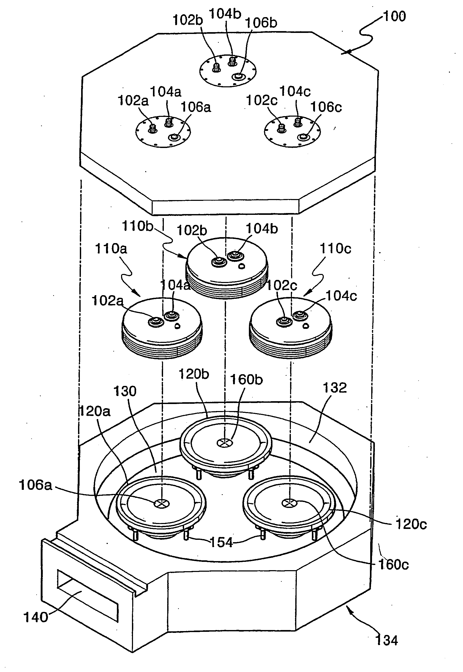
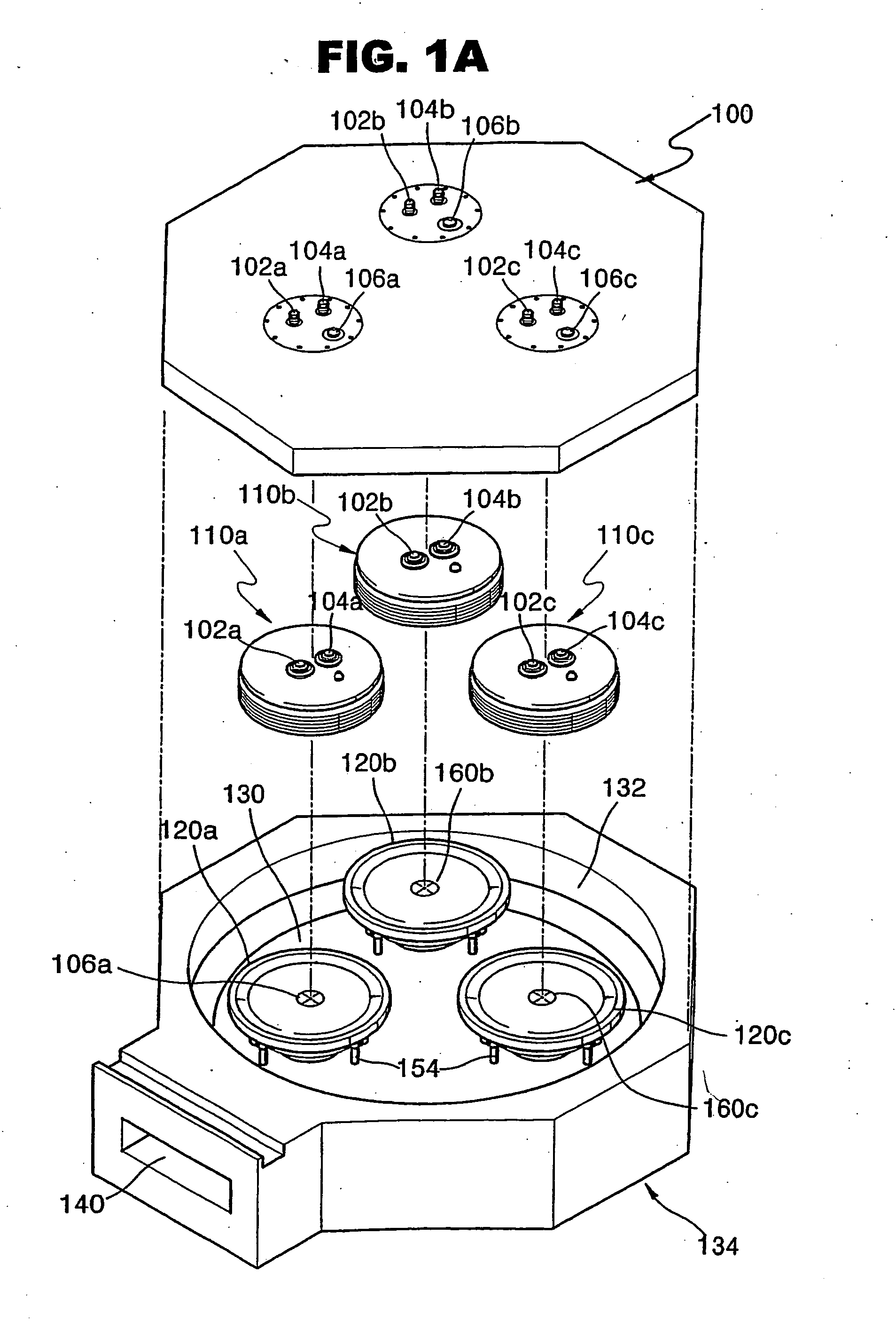
FIG. 1A is a schematic drawing of an apparatus for forming thin films having three independent reactors according to the first embodiment of the present invention.
Referring to FIG. 1A, the chamber 100 and 135 is equipped with three independent single substrate type of reactors for depositing a thin film on the surface of each substrate in each reactor. In the following description only one reactor is considered unless specified otherwise because the reactors are identical. Each reactor has a reactor upper body 110a, 110b, 110c, a reactor lower body 120a, 120b, 120c, and a supporting pin 160a, 160b, 160c which is mounted in the reactor lower body 120a, 120b, 120c, and the inferior of a reactor is defined by a reactor upper body 110, 110b, 110c and a reactor lower body 120a, 120b, 120c. The reactor upper body 110a, 110b, 110c is fixed to the chamber cover 100, wherein the reactor is equipped with a gas inlet 102a, 102b, 102c and a gas outlet 104, 104b, 104c which are the passageways...
embodiment 2
FIG. 2A is a schematic drawing of a top view of a thin film formation apparatus according to the present invention as a second embodiment. FIG. 2B is a cross-sectional drawing of FIG. 2A along the dotted line A-A′. Here, FIG. 2A is an illustration of the top view of a reactor without the chamber cover 100 as well as the reactor upper bodies 110. Therefore, the description of the chamber cover 100 (not shown) and the reactor upper bodies 110 (not shown) are omitted here, since they are identical to those in Embodiment 1.
Referring to FIG. 2A, underneath the substrate susceptor (not shown) in the reactor lower body 220a, 220b, 220c (only singular is used for the descriptions to follow), a heater (not shown) for heating the substrate is installed. The reactor lower body 220a, 220b, 220c moves up and down, therefore a substrate is loaded or unloaded when the reactor lower body is in “low” position. Once a substrate to be processed is safely loaded onto the susceptor of the reactor lowe...
embodiment 3
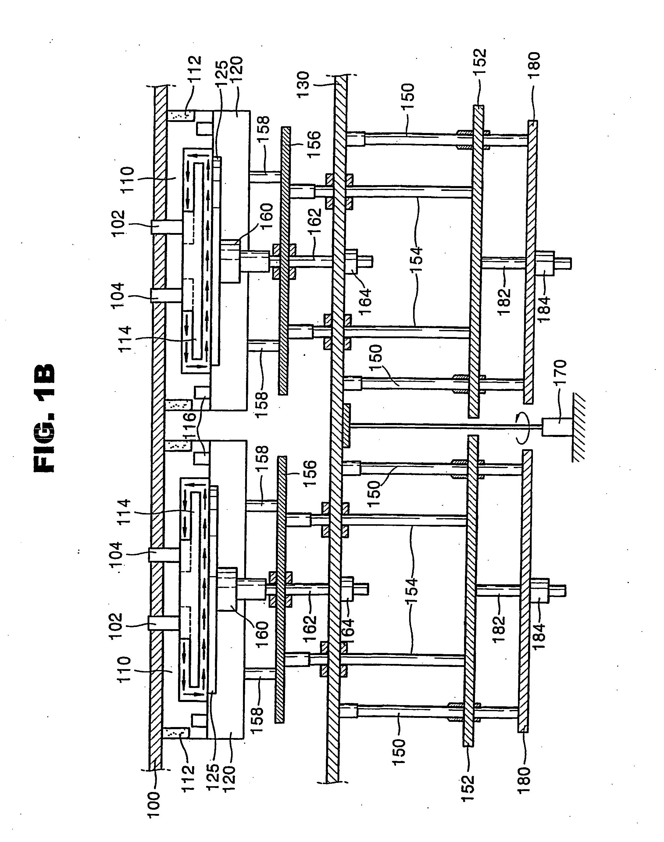
In Embodiment 2, the arm axis 292 moves in three ways; up and down motion and a rotational motion referring to FIGS. 2A and 2B. Instead, a substrate (not shown) can be loaded and unloaded by changing the arm axis 292 movement to rotational motion only, and also by changing the movement of the substrate supporting pin 272 to up and down motion actively by installing a center drive motor 286 as illustrated in FIG. 2C according to the present invention. A similar illustration on the substrate supporting pin 160 with a center drive motor 164 is as shown in FIG. 1B.
A deposition apparatus according to the exemplary Embodiment 3 is illustrated in FIG. 2A. The substrate supporting pin 272 in FIG. 2B moves up and down passively, but in FIG. 2C. the substrate supporting pin 272, and associated center shaft 274 moves up and down actively by the center drive motor 288 such as a air pressure cylinder attached to the bottom of the center shaft 274 and the substrate supporting pin 272. FIG. 2C ...
PUM
| Property | Measurement | Unit |
|---|---|---|
| Fraction | aaaaa | aaaaa |
| Diameter | aaaaa | aaaaa |
| Height | aaaaa | aaaaa |
Abstract
Description
Claims
Application Information