

Bump transfer fixture
a technology of bump transfer and fixture, which is applied in the field of bump transfer process, can solve the problems of contaminating the environment with solvents for printing or electrolytic plating, affecting the reliability of the chip package structure, and expensive processes and are difficult to control, so as to simplify the bump transfer process and reduce the cost of the process
- Summary
- Abstract
- Description
- Claims
- Application Information
AI Technical Summary
Benefits of technology
Problems solved by technology
Method used
Image

Examples
first embodiment
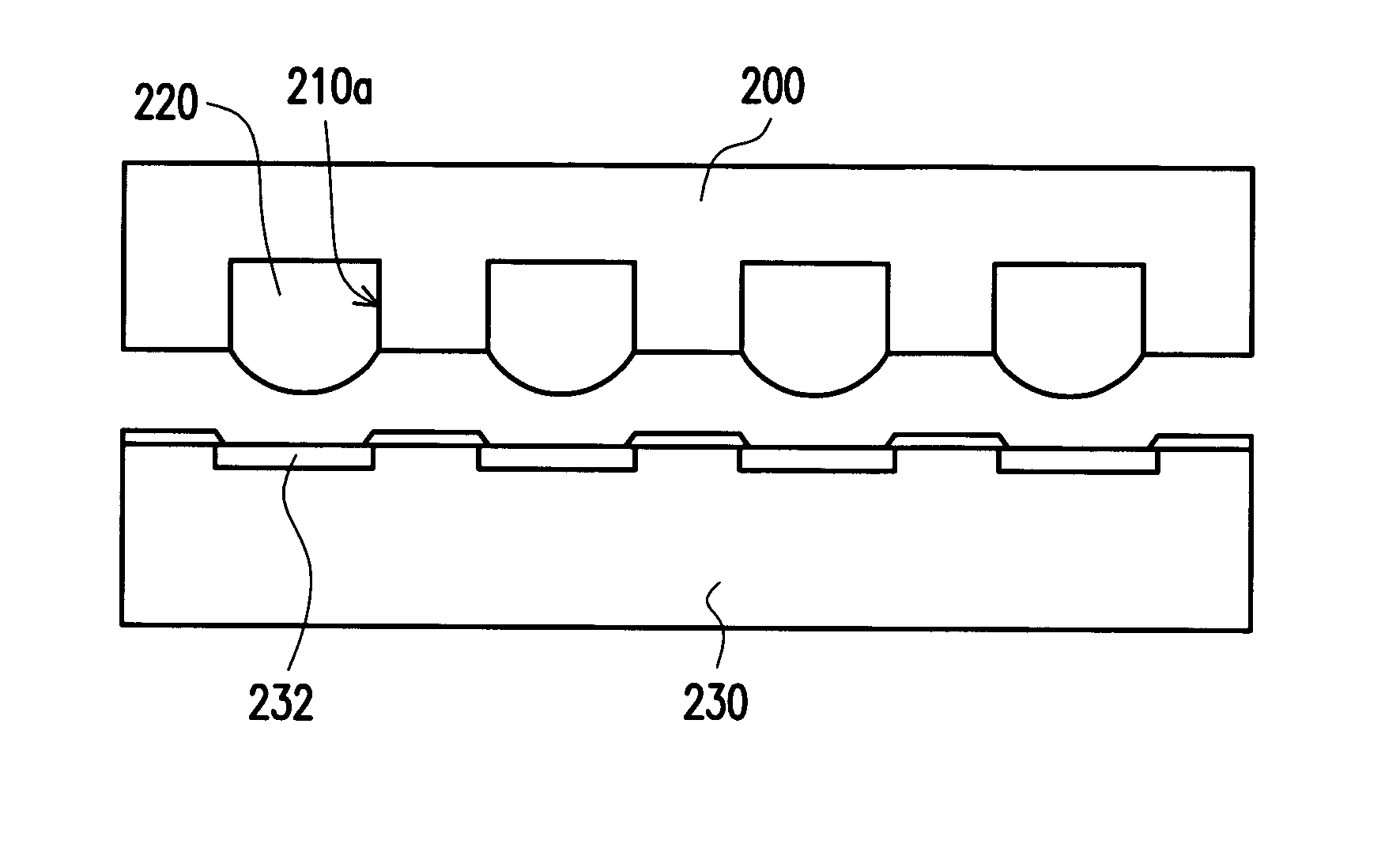
[0023] Referring to FIG. 2C, a carrier 230 is placed below the transfer plate 200. Then the transfer plate 200 is flipped upside-down to make the solder bumps face toward the carrier 230. In the first embodiment, the carrier 230 is a wafer or a substrate. The carrier 230 has a plurality of bump pads 232 on its surface. The bump pads 232 correspond to the concaves 210a and the solder bumps 220 respectively. Then the solder bumps 220 are melted so that the solder bumps 220 leave the fix structures 210a due to the gravity and are transferred to the bump pads 232 of the carrier 230. Referring to FIG. 2D, after the bump transfer process is finished, the solder bumps 220 are formed on the bump pads 232 of the carrier 230.
[0024] Referring to FIG. 2C, the solder bumps 220 can be melted by melting at a high temperature or using laser to heat up the solder bumps 220. Furthermore, the cohesive force of the solder bumps will reduce the adhesive force between the solder bumps 220 and the fix str...
second embodiment
[0027] Referring to FIG. 3C, a carrier 230 is placed below the transfer plate 200b. Then the transfer plate 200b is flipped upside-down to make the solder bumps face toward the carrier 230. In the second embodiment, the carrier 230 is a wafer or a substrate. The carrier 230 has a plurality of bump pads 232 on its surface. The bump pads 232 correspond to the fix structures 210b and the solder bumps 220a respectively. Then the solder bumps 220a are melted so that the solder bumps 220a leave the convexes 210b due to the gravity and are transferred to the bump pads 232 of the carrier 230. Referring to FIG. 3D, after the bump transfer process is finished, the solder bumps 220a are formed on the bump pads 232 of the carrier 230.
[0028] Referring to FIG. 3C, the solder bumps 220a can be melted by melting at a high temperature or using laser to heat up the solder bumps 220a. Furthermore, the cohesive force of the solder bumps will reduce the adhesive force between the solder bumps 220a and t...
PUM
 Abstract
Description
Claims
Application Information