Circuit for inspecting semiconductor device and inspecting method

a semiconductor device and circuit technology, applied in the field of circuits for inspecting semiconductor devices and inspecting methods, can solve the problems of inability to carry out a quality inspection by an actual display in this case, and spend a lot of cost on a module which is determined to be defective, and achieves efficient quality inspection, high definition, and efficient inspection of the display device

Inactive Publication Date: 2005-02-17
SEMICON ENERGY LAB CO LTD
View PDF18 Cites 18 Cited by
  • Summary
  • Abstract
  • Description
  • Claims
  • Application Information

AI Technical Summary

Benefits of technology

[0020] According to the invention, a determination can be performed in the state of a TFT substrate without performing an inspection by looking at an actual test pattern display, therefore, an efficient quality inspection can be performed quite simply by a small-scale inspecting circuit.
[0021] Specifically, determination of a circuit operation can be performed in a various display devices such as an LCD, an EL display, and a plasma display which use a digital signal as a video signal. Further, an inspection can be p...

Problems solved by technology

According to this method, however, an inspection is carried out in the phase that a display device itself is almost completed as the module 1200, therefore, there is a defect that much cost is spent on a module which is determined to be defective.
That is, since a defect due to a circuit defect originates in the TFT substrate 1201 only, the process ...

Method used


Image

  • Circuit for inspecting semiconductor device and inspecting method
  • Circuit for inspecting semiconductor device and inspecting method
  • Circuit for inspecting semiconductor device and inspecting method

Examples


embodiment

[0040] [Embodiment Mode 1]

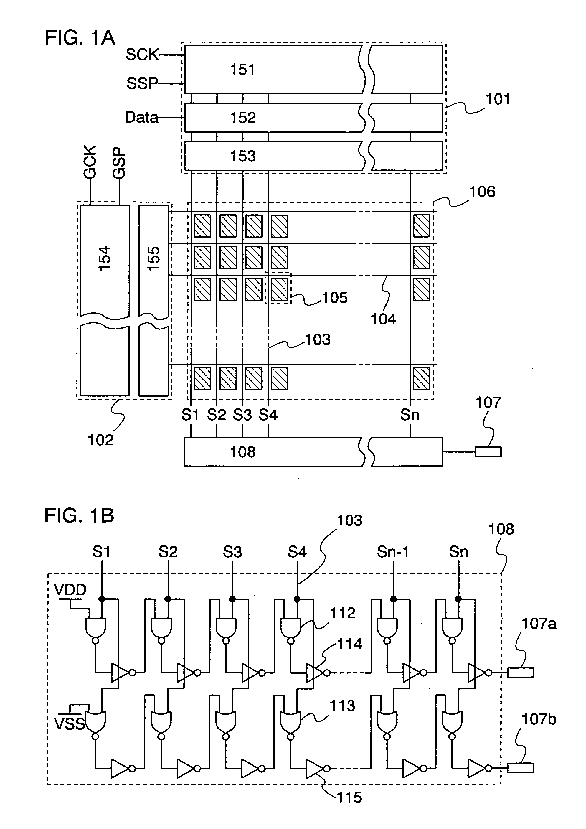
[0041]FIG. 1A shows an embodiment mode of the invention. A source driver 101, a gate driver 102, a pixel region 106, an inspecting circuit 108, and an inspecting output terminal 107 are formed over a substrate. The pixel region 106 comprises a plurality of pixels 105 are formed in matrix, and each of the pixels is controlled by a source signal line 103 and a gate signal line 104.

[0042] The source driver 101 comprises a shift register and a NAND 151, a data latch 152, a level shifter and a buffer 153, and the gate driver 102 comprises a shift register and a NAND 154, a level shifter and a buffer 155. However, no restriction is imposed upon the configuration of the display device here.

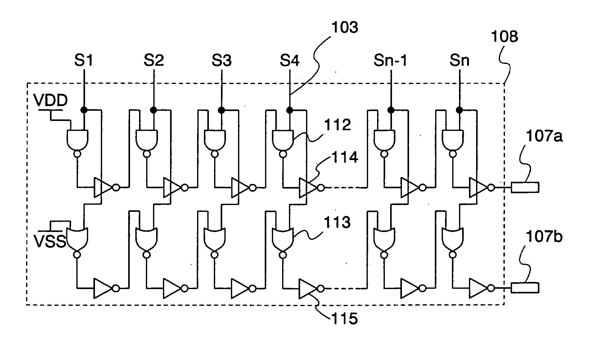
[0043] A configuration of the inspecting circuit is shown in FIG. 1B. In the inspecting circuit 108, circuits connected to each source signal line 103, in which a plurality of NANDs 112 and a plurality of inverters 114 are connected alternately in series, and circuits connecte...


PUM


Abstract

It is configured by plurality of NAND circuits connected in series through a plurality of inverters, and a plurality of NOR circuits connected in series through the plurality of inverters. Each of a plurality of source signal lines provided in a pixel portion is connected to one input terminal of a NAND circuit and a NOR circuit, and an output of an inspection is obtained from final lines of the NAND circuit and the NOR circuit connected in series. In this manner, an inspecting circuit which is capable of determining a defect simply and accurately by using a small-scale circuit, and a method thereof are provided.

Description

TECHNICAL FIELD [0001] The present invention relates to an inspecting circuit provided in a display device having a pixel region in which pixels are arranged in matrix, and an inspecting method of the display device. Further, the invention relates to an inspecting circuit and an inspecting method of a semiconductor device having a pixel region in which pixels are arranged in matrix. BACKGROUND ART [0002] A display device such as a liquid crystal display (LCD) and an electroluminescence (EL) display has been advanced in size and definition in recent years. Furthermore, high integration of circuits is also advanced by forming a pixel portion and peripheral circuitry for controlling the pixel portion integrally on a substrate. [0003] In the case where element breakdown occurs due to patterning defects, electrostatic discharge (ESD) event and the like in the manufacturing process, a normal operation of the display device as a whole cannot be obtained, therefore, they are required to be ...

Claims


Application Information

Patent Timeline
IPC IPC(8): G01R31/28G09G3/00G09G3/20
CPCG01R31/2853G09G2330/12G09G3/20G09G3/006
Inventor TANADA, YOSHIFUMI
Owner SEMICON ENERGY LAB CO LTD
Why Eureka
Try Eureka