Semiconductor device having a data latching or storing function

a technology of latching or storing function and semiconductor devices, which is applied in the direction of information storage, static storage, digital storage, etc., can solve the problems of data storage being lost, increasing leakage current, and exposing the dilemma of increasing speed and reducing power consumption, so as to achieve the effect of reducing power consumption

Active Publication Date: 2005-02-17
TEXAS INSTR INC
View PDF8 Cites 35 Cited by
  • Summary
  • Abstract
  • Description
  • Claims
  • Application Information

AI Technical Summary

Benefits of technology

[0008] An advantage of the invention is providing a

Problems solved by technology

If the application of source voltage VDD is stopped, the supply of a data latch current to the data storage node on the side where an H-level voltage is clamped is stopped, and the data stored will be lost.
However, in recent

Method used


Image

  • Semiconductor device having a data latching or storing function
  • Semiconductor device having a data latching or storing function
  • Semiconductor device having a data latching or storing function

Examples


Embodiment Construction

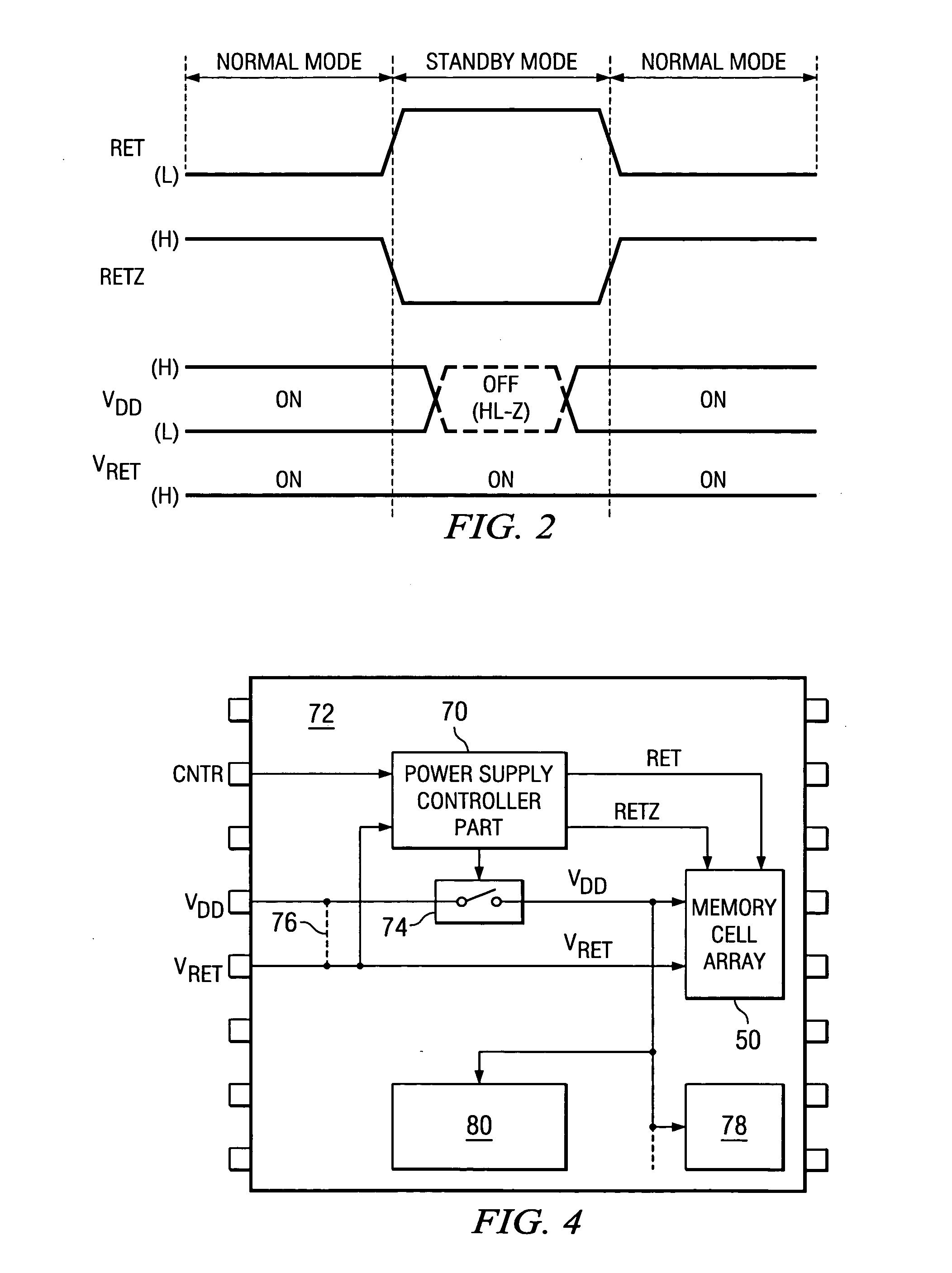
[0014] With the semiconductor device of the present invention, the current consumed in latching data and during the standby can be significantly decreased in order to realize reduced power consumption.

[0015] Suitable embodiments of the present invention will be explained below with reference to the attached drawings.

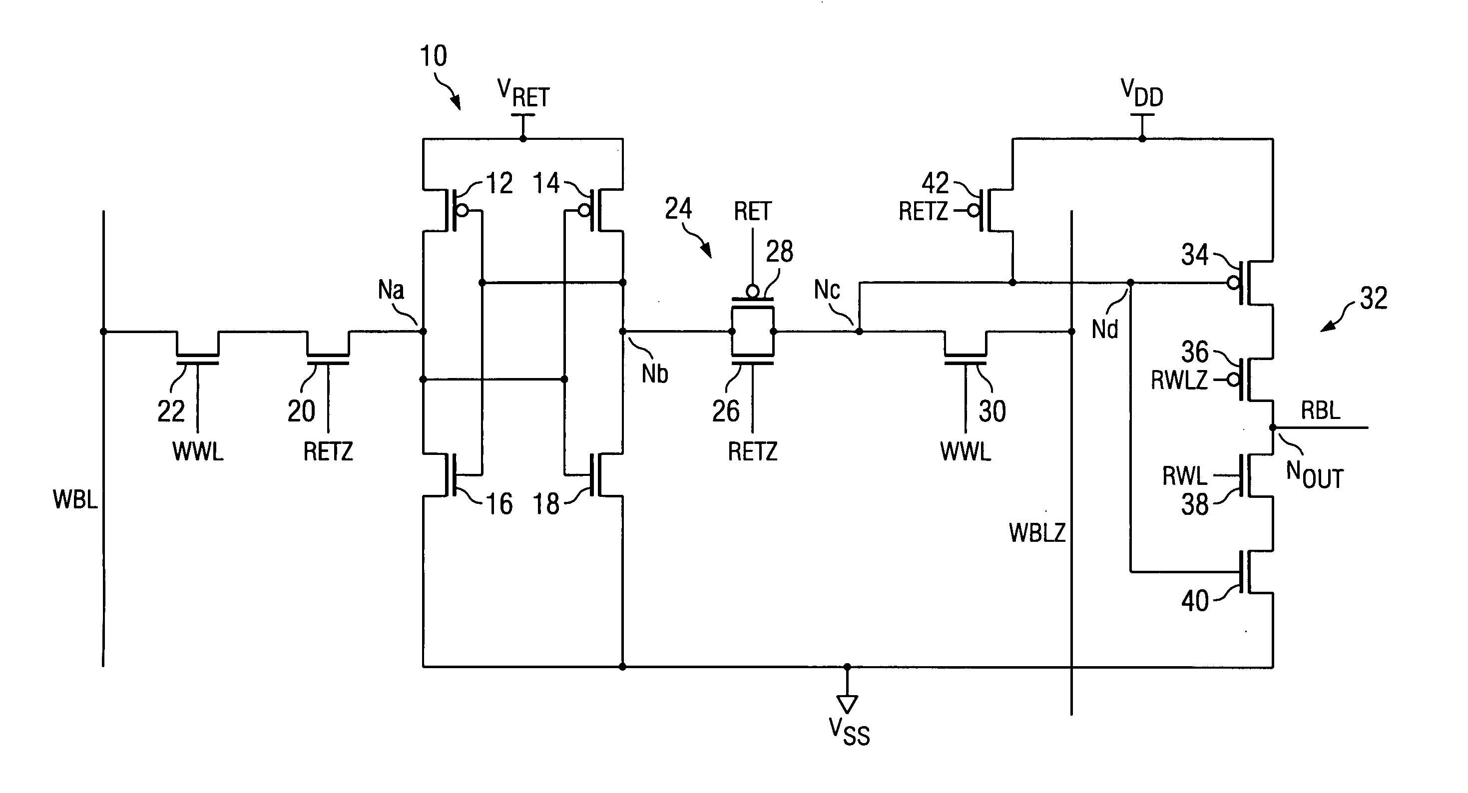
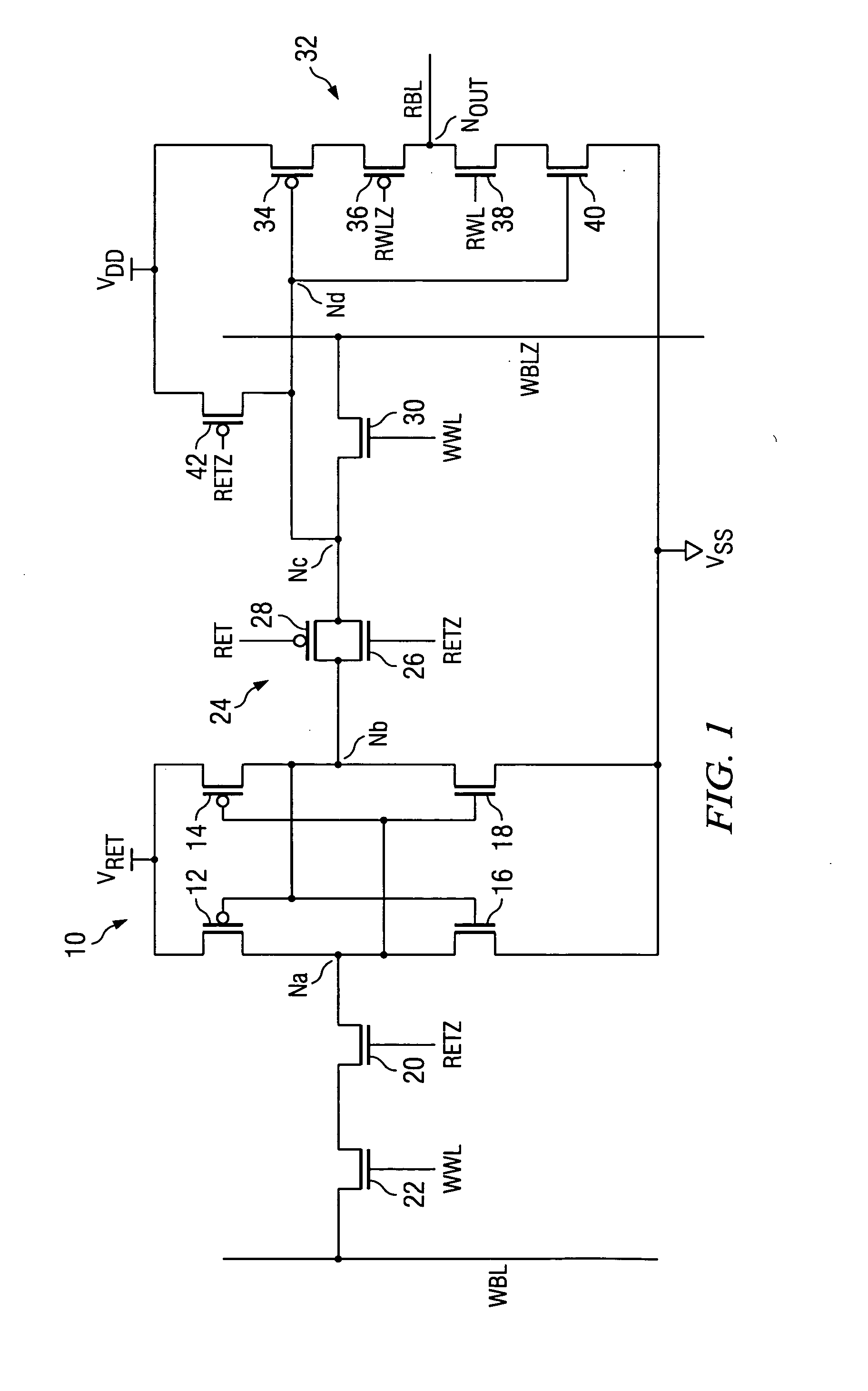
[0016] The circuit configuration of a static RAM in accordance with an embodiment of the present invention is shown in FIG. 1. Said memory is configured as an asynchronous two-port (one write port and one read port) memory cell, and it is connected to one word line WWL and a pair of write bit lines WBL and WBLZ as well as a pair of read word lines RWL and RWLZ and 1-bit read line RBL.

[0017] Latch circuit 10 of said memory cell is configured using a pair of CMOS inverters, that is, two PMOS transistors 12 and 14, and two NMOS transistors 16 and 18. More specifically, while the respective power supply terminals of PMOS transistors 12 and 14 are connected to a source vol...


PUM


Abstract

The current consumed by latching data and during standby are significantly decreased in order to realize reduced power consumption. In this memory cell, source voltages VRET and VDD are supplied to latch circuit 10 and output circuit 32 from different systems. Latch circuit 10 can be separated from a peripheral circuit by NMOS transistor 20 and transmission gate 24. MOS transistors 12, 14, 16, and 18, which constitute latch circuit 10 and MOS transistors 20, 26, and 28, which constitute the switch circuit, are configured using low-leakage MOS transistors with leakage current significantly lower than those of standard MOS transistors used to configure the peripheral circuit including output circuit 32.

Description

FIELD OF THE INVENTION [0001] The present invention pertains to a semiconductor device having a data latching or storing function. In particular, it pertains to a semiconductor memory device and a semiconductor memory cell capable of latching data continuously while a source voltage is applied. BACKGROUND OF THE INVENTION [0002] Although a static RAM (Random-Access Memory) has the disadvantage that many elements are needed to configure each memory cell, it has the advantage that it stores data continuously without requiring a refresh operation as long as a source voltage is applied so as to achieve a high-speed writing / reading. In general, in the case of a static RAM, a pair of CMOS (Complementary Metal Oxide Semiconductor) inverters are used to configure each flip-flop circuit. More specifically, two CMOS inverters, each configured by connecting a PMOS (P-channel MOS) transistor and an NMOS (N-channel MOS) transistor in series, are connected in parallel between a source voltage ter...

Claims


Application Information

Patent Timeline
IPC IPC(8): G11C11/41G11C7/00G11C8/00G11C11/34G11C11/419
CPCG11C2207/2227G11C11/419
Inventor SHIRAISHI, ATSUSHI
Owner TEXAS INSTR INC
Why Eureka
Try Eureka