Semiconductor memory device and manufacturing method thereof

a semiconductor and memory technology, applied in the direction of semiconductor devices, electrical devices, transistors, etc., can solve the problems of memory data error, difficult to obtain well-controlled traps, etc., and achieve the effect of reliably retaining electrons trapped

Active Publication Date: 2005-02-17
FUJITSU LTD
View PDF14 Cites 19 Cited by
  • Summary
  • Abstract
  • Description
  • Claims
  • Application Information

AI Technical Summary

Benefits of technology

In view of the foregoing, it is an object of the present invention to provide a semicondu...

Problems solved by technology

It is, however, difficult to obtain well-controlled traps having an intended depth, capture cross-section, capture rate, and emission rate.
Also, electron...

Method used


Image

  • Semiconductor memory device and manufacturing method thereof
  • Semiconductor memory device and manufacturing method thereof
  • Semiconductor memory device and manufacturing method thereof

Examples


Embodiment Construction

Preferred embodiments of the present invention will be described below with reference to the accompanying drawings, wherein like reference numerals refer to like elements throughout.

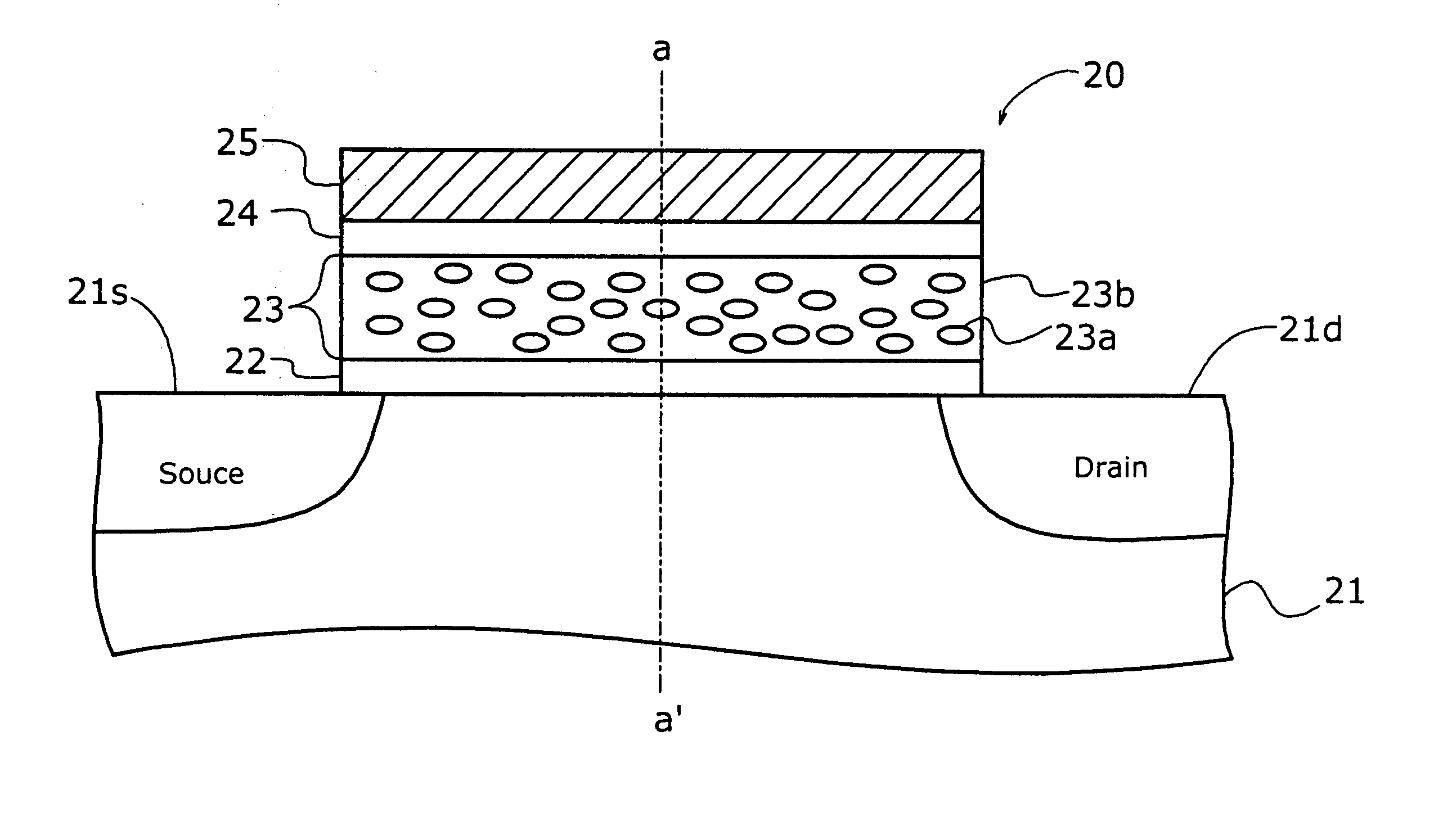
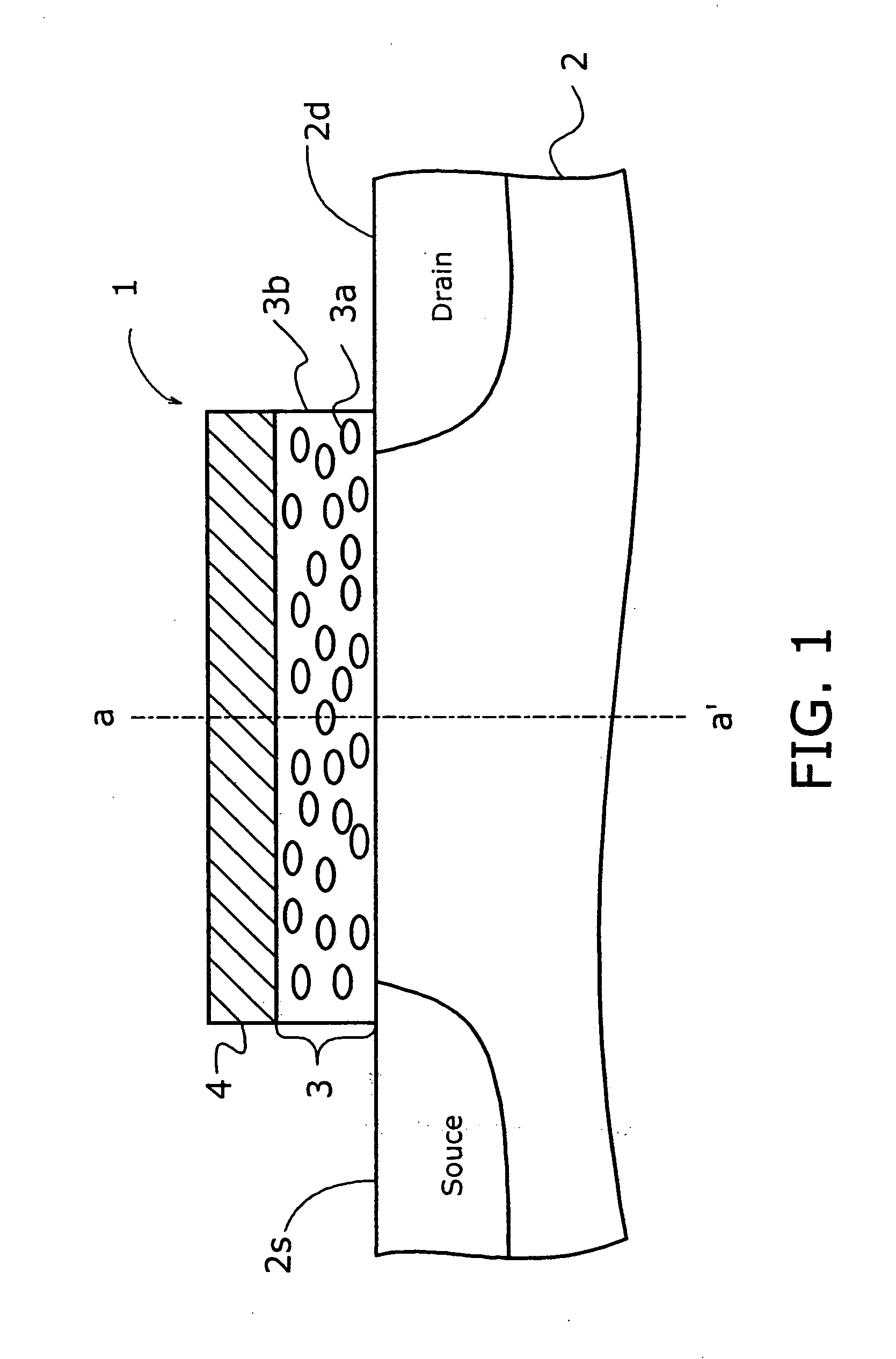
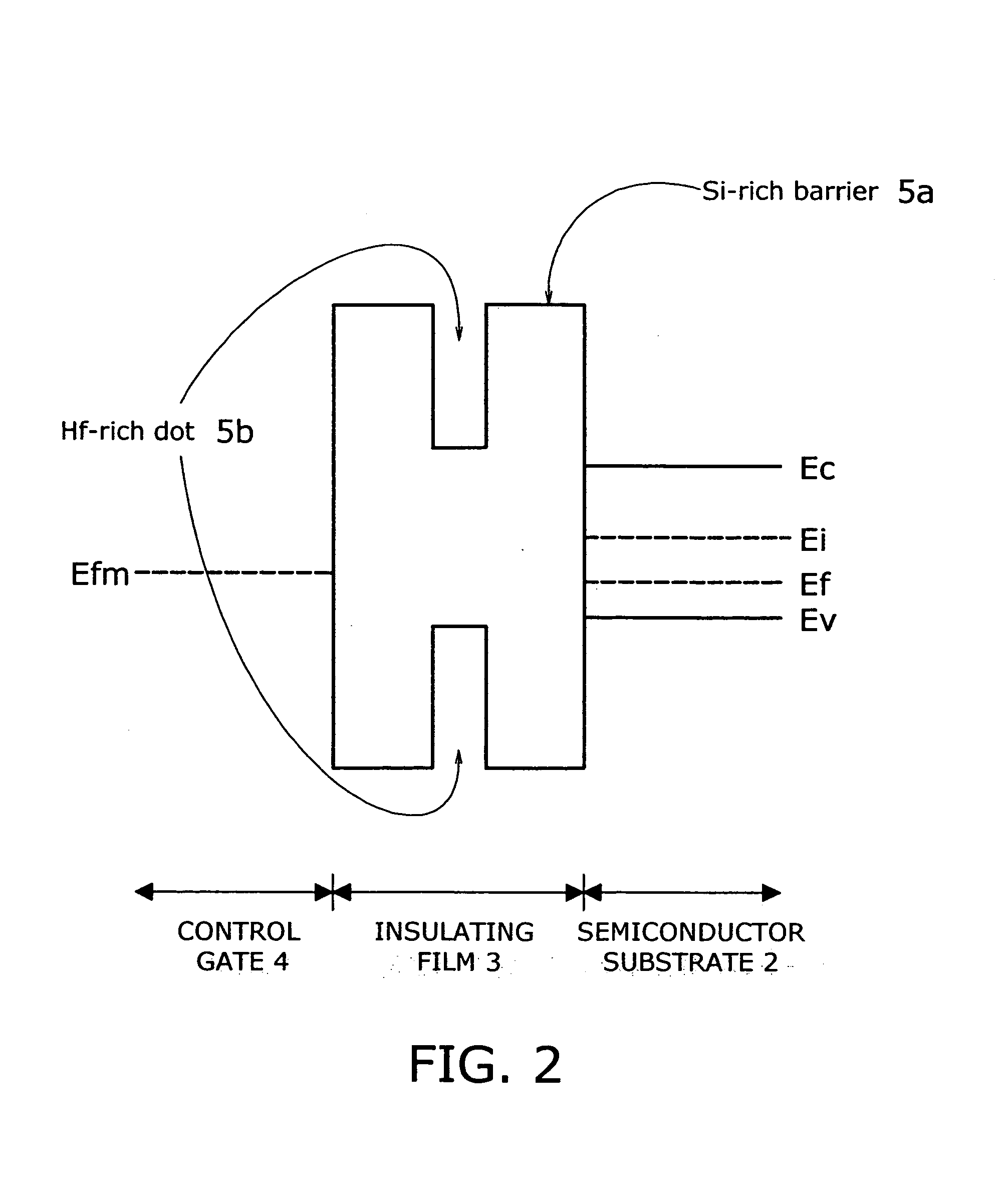
FIG. 1 is a simplified cross-sectional view of a semiconductor memory cell according to a first embodiment of the present invention. While a semiconductor memory device actually contains a number of memory cells, FIG. 1 shows only one such memory cell for the purpose of explanation. The illustrated semiconductor memory cell 1 is constructed on a p-type semiconductor substrate 2. A source region 2s and a drain region 2d are formed in a surface region of the semiconductor substrate 2. Then a high-dielectric gate insulating film 3 is formed on top of the semiconductor substrate 2, covering the channel region between the source region 2s and drain region 2d. Deposited on top of the high-dielectric gate insulating film 3 is a control gate 4.

Here, the semiconductor substrate 2 is a silicon substrate, and i...


PUM


Abstract

A semiconductor memory device which more reliably retains electrons trapped in its charge-trapping regions. A high-dielectric gate insulating film is grown on a semiconductor substrate. This gate insulating film is composed of first and second oxides, where the second oxide has a smaller bandgap than that of the first oxide and is scattered in dot-like form, surrounded by the first oxide. The memory cell is programmed by injecting electrons into a local potential minimum that is produced due to the bandgap difference between the phase-separated first and second oxides.

Description

CROSS-REFERENCE TO RELATED APPLICATIONS This application is based upon and claims priority of Japanese Patent Application No. 2002-87301, filed on Mar. 27, 2002, the contents being incorporated herein by reference. This is a Divisional of application Ser. No. 10 / 364,387 Filed Feb. 12, 2003. BACKGROUND OF THE INVENTION 1. Field of the Invention The present invention relates to a semiconductor memory device, and more particularly to a non-volatile semiconductor memory device with a high-dielectric gate insulating film. 2. Description of the Related Art Metal-oxide-semiconductor field-effect transistors (MOSFETs) are widely used in integrated circuits, particularly including memory devices for storing digital data, such as electrically erasable programmable read-only memory (EEPROM) and flash memory. Cellular phones, for example, employ this kind of semiconductor memory chips as their firmware code storage, and personal computers have one on their motherboard to store the basic in...

Claims


Application Information

Patent Timeline
IPC IPC(8): H01L21/28H01L27/115H01L21/8247H01L29/51H01L29/788H01L29/792
CPCH01L21/28185H01L21/28194H01L21/28202H01L21/28282H01L27/115H01L29/792H01L29/513H01L29/515H01L29/517H01L29/518H01L29/511H01L29/40117H10B69/00
Inventor SUGIYAMA, YOSHIHIRO
Owner FUJITSU LTD
Why Eureka
Try Eureka