LCD device including a TFT for reducing leakage current

a technology of lcd device and tft, which is applied in the direction of semiconductor devices, identification means, instruments, etc., can solve problems such as difficulties in achieving, and achieve the effect of suppressing the increase of tft area and reducing the leakage current of

Active Publication Date: 2005-02-24
HANNSTAR DISPLAY CORPORATION
View PDF0 Cites 48 Cited by
  • Summary
  • Abstract
  • Description
  • Claims
  • Application Information

AI Technical Summary

Benefits of technology

[0015] In view of the above problem in the conventional LCD device, it is an object of the present invention to provide an LCD...

Problems solved by technology

However, this technique involves a problem in that TFTs 230, black matrix 242 and coloring...

Method used


Image

  • LCD device including a TFT for reducing leakage current
  • LCD device including a TFT for reducing leakage current
  • LCD device including a TFT for reducing leakage current

Examples


Embodiment Construction

[0039] Now, the present invention is more specifically described with reference to accompanying drawings, wherein similar constituent elements are designated by similar reference numerals.

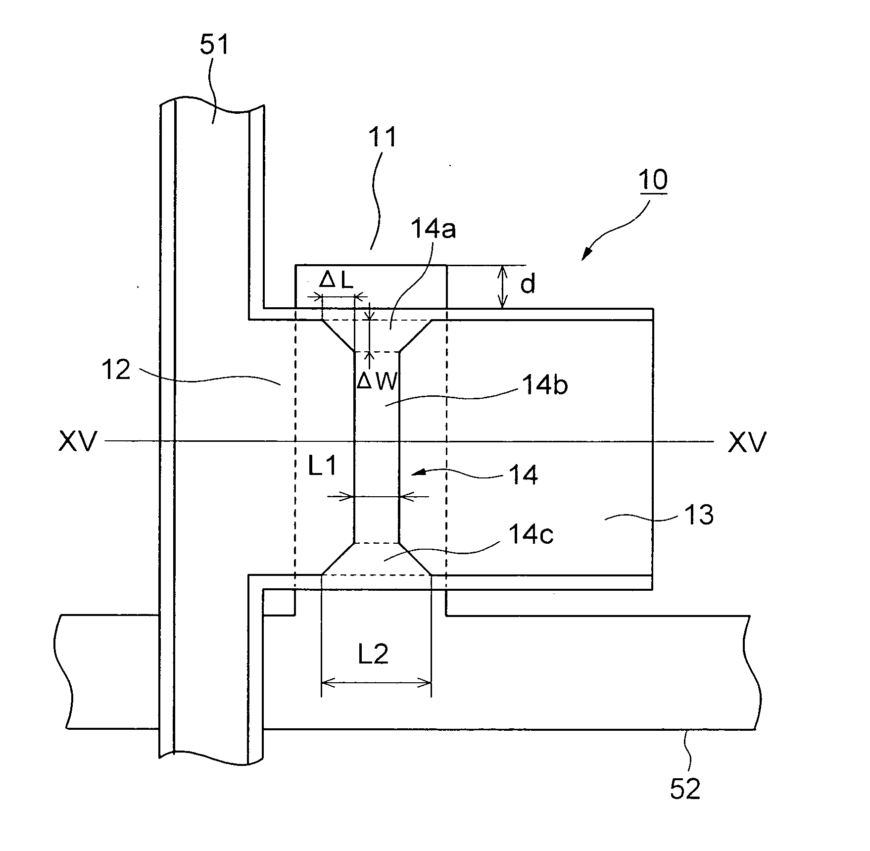
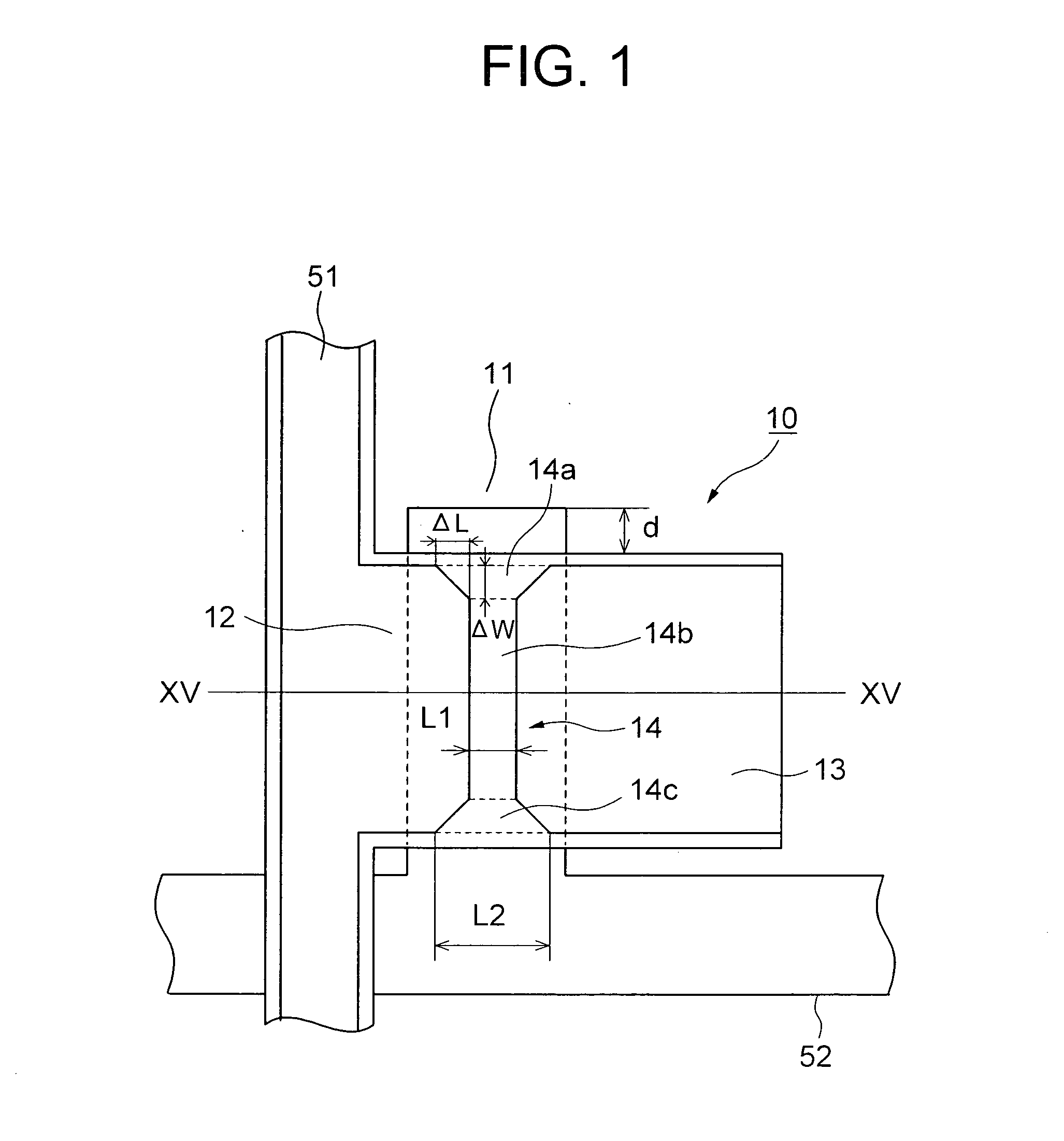
[0040]FIG. 1 shows a TFT generally designated by numeral 10 and formed on a TFT substrate in an LCD device according to a first embodiment of the present invention. The TFT 10 includes a drain electrode 12, a source electrode 13, a gate electrode 11 and a channel (channel region) 14, which are somewhat different from those shown in FIG. 16. It is to be noted that the TFT 10 has a sectional structure similar to that of the TFT shown in FIG. 15.

[0041] The structure shown in FIG. 15 corresponds to the structure taken along line XV-XV in FIG. 1. The TFT 10 shown in FIG. 1 is disposed in the vicinity of the intersection between a signal line and a scanning line, such as 231 and 232 shown in FIG. 14. The LCD device of the present embodiment has structures other than the structure of the TFT which are s...


PUM


Abstract

An amorphous-silicon TFT (thin-film-transistor) in an LCD device has a larger channel length at both the edge portions of the channel of the TFT compared to the central portion of the channel by forming chamfers at the corners of the source and drain electrodes. The larger channel length at both the edge portions reduces the leakage current caused by the turned-around light incident onto the channel.

Description

FIELD OF INVENTION [0001] The present invention relates to an LCD device including a thin-film-transistor (TFT) and, more particularly, to the structure of the TFT used in the LCD device. The present invention also relates to a method for manufacturing a TFT in an LCD device. BACKGROUND TECHNOLOGY [0002] Active-matrix LCD devices including active elements such as TFTs as switching devices have been increasingly used. Materials used for the semiconductor layers of the TFTs in the LCD device include polysilicon (p-Si) and amorphous silicon (a-Si), for example. A TFT having a polysilicon layer is herein referred to as a p-Si TFT whereas a TFT having an amorphous silicon layer is herein referred to as an a-Si TFT. Comparing both the TFTs against each other, the a-Si TFT has advantages of a smaller number of fabrication steps and allowing lower-temperature fabrication steps. [0003]FIG. 13 shows the sectional view of an LCD panel in a general LCD device, wherein a-Si TFTs 230 are fabricat...

Claims


Application Information

Patent Timeline
IPC IPC(8): G02F1/1368G09F9/30H01L21/336H01L29/417H01L29/786
CPCG02F1/1368
Inventor HASHIMOTO, YOSHIAKIKIMURA, SHIGERUSUZUKI, SEIJI
Owner HANNSTAR DISPLAY CORPORATION
Why Eureka
Try Eureka