Lithographic apparatus and device manufacturing method

Active Publication Date: 2005-02-24
ASML NETHERLANDS BV
View PDF35 Cites 271 Cited by
  • Summary
  • Abstract
  • Description
  • Claims
  • Application Information

AI Technical Summary

Benefits of technology

Accordingly, it would be advantageous, for example, to provide accura

Problems solved by technology

For example, because of the required small size of the features of a sensor, if a galvanic cell is allowed to be

Method used


Image

  • Lithographic apparatus and device manufacturing method
  • Lithographic apparatus and device manufacturing method
  • Lithographic apparatus and device manufacturing method

Examples


embodiment 1

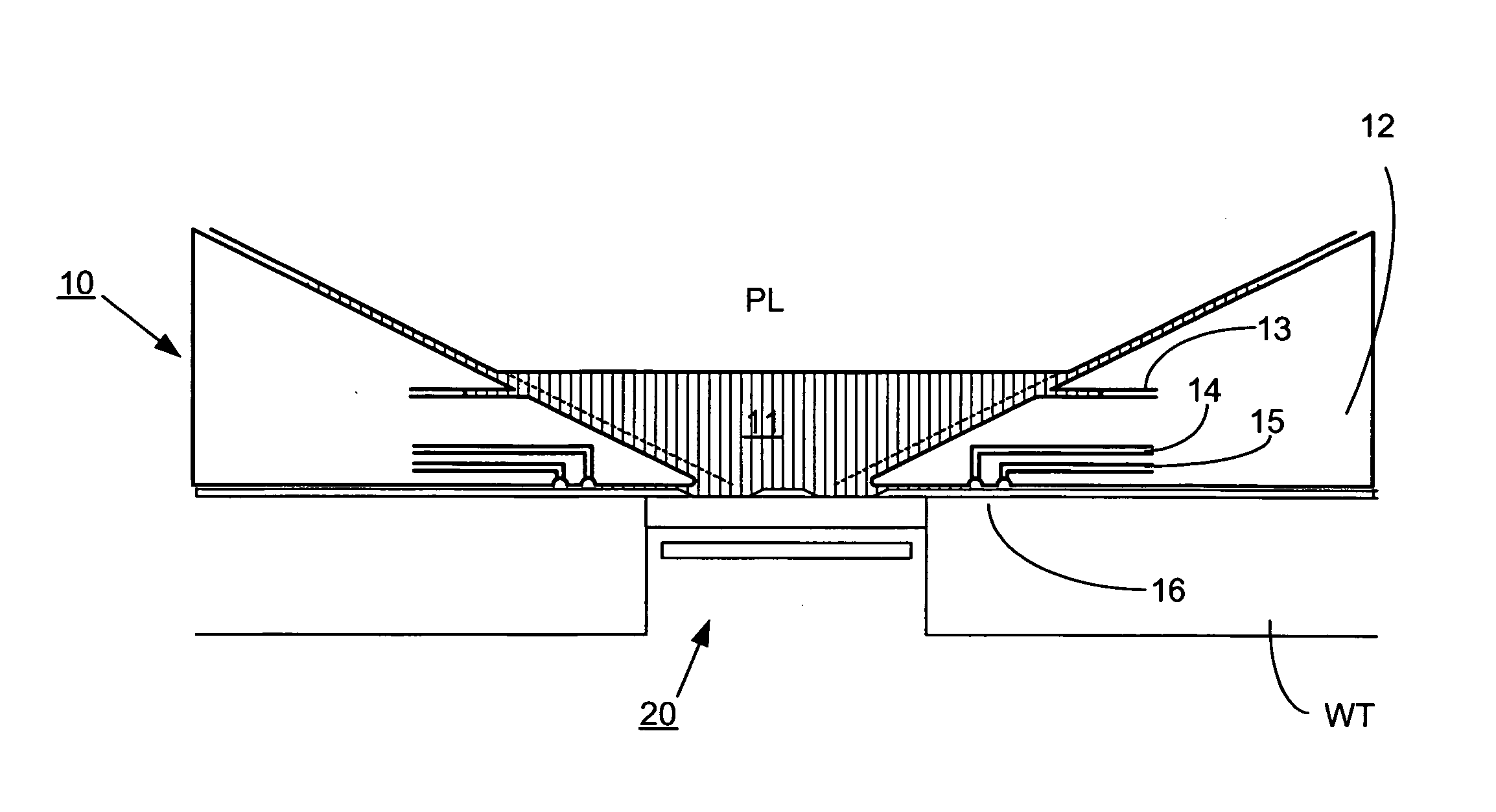
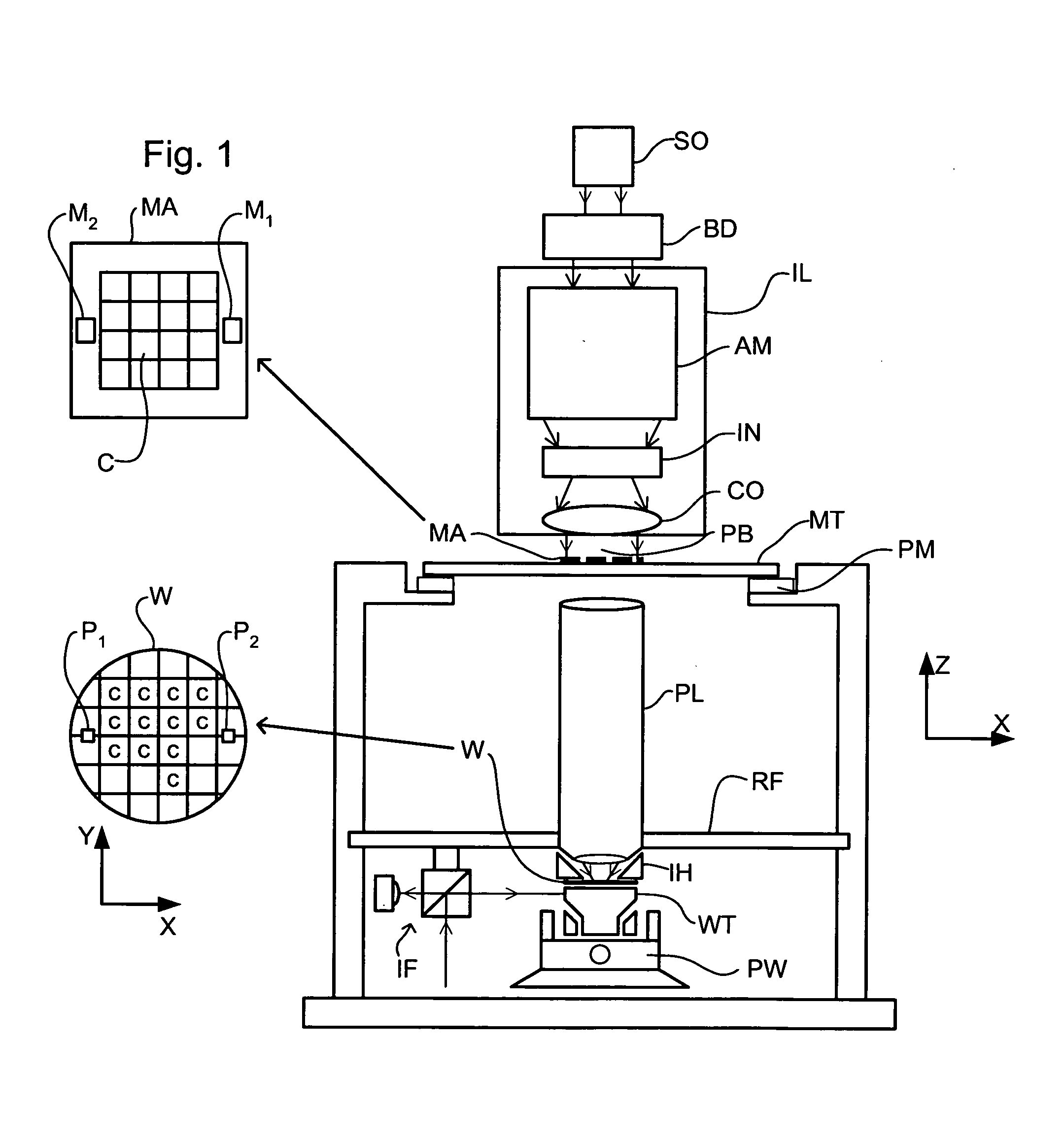
FIG. 1 schematically depicts a lithographic apparatus according to one embodiment of the invention. The apparatus comprises: an illumination system (illuminator) IL configured to condition a radiation beam PB (e.g. UV radiation or DUV radiation). a support structure (e.g. a mask table) MT constructed to support a patterning device (e.g. a mask) MA and connected to a first positioner PM configured to accurately position the patterning device in accordance with certain parameters; a substrate table (e.g. a wafer table) WT constructed to hold a substrate (e.g. a resist-coated wafer) W and connected to a second positioner PW configured to accurately position the substrate in accordance with certain parameters; and a projection system (e.g. a refractive projection lens system) PL configured to project a pattern imparted to the radiation beam PB by patterning device MA onto a target portion C (e.g. comprising one or more dies) of the substrate W.

The illumination system may include v...

embodiment 2

A second embodiment will now be described with reference to FIG. 7 and is the same as the first embodiment except as described below.

In the second embodiment, the absorption element 100 comprises two metal layers 105, 107. However, in the second embodiment, the isolation layer 120 is made of an electrical insulation material and is sandwiched between the first and second layers 105, 107. Again, the isolation layer is only necessary where the stack of layers 105 and 107 would, without it, come into contact with the immersion liquid but, in an implementation, a continuous isolation layer is used to deal with imperfections in layer 105. Thus, the surface of the absorption element 100 is formed partly of the first metal layer 105 and partly of the layer of insulation material 120. In this embodiment the function of the layer of insulation material 120 is to electrically isolate the first and second metal layers 105, 107 from each other such that no galvanic couple exists. In this emb...

embodiment 3

A third embodiment will now be described with reference to FIG. 8 and is the same as the first embodiment save as described below.

In the third embodiment, there is no layer of insulation material 120. There are two layers 105, 108, one of which is a metal layer 105, for example Cr, and another of which is a non-metal layer 108, such as a ceramic, for example a metal carbide or nitride such as TiN. The layers 105, 108 may be either way around. This combination also has good resistance to galvanic corrosion and has an advantage of being easy to manufacture as each layer needs only to be about 100 nm thick.


PUM


Abstract

In a lithographic projection apparatus, a liquid supply system maintains liquid in a space between a projection system of the lithographic projection apparatus and a substrate. A sensor positioned on a substrate table, which holds the substrate, is configured to be exposed to radiation when immersed in liquid (e.g., under the same conditions as the substrate will be exposed to radiation). By having a surface of an absorption element of the sensor, that is to be in contact with liquid, formed of one or fewer metal types, long life of the sensor may be obtained.

Description

This application claims priority from European patent application EP 03255228.3, filed Jul. 24, 2003, which is incorporated herein in its entirety. FIELD The present invention relates to a lithographic apparatus and a method for manufacturing a device. BACKGROUND A lithographic apparatus is a machine that applies a desired pattern onto a substrate, usually onto a target portion of the substrate. A lithographic apparatus can be used, for example, in the manufacture of integrated circuits (ICs). In that instance, a patterning device, which is alternatively referred to as a mask or a reticle, may be used to generate a circuit pattern to be formed on an individual layer of the IC. This pattern can be transferred onto a target portion (e.g. comprising part of, one, or several dies) on a substrate (e.g. a silicon wafer). Transfer of the pattern is typically via imaging onto a layer of radiation-sensitive material (resist) provided on the substrate. In general, a single substrate will c...

Claims


Application Information

Patent Timeline
IPC IPC(8): G03F7/20H01L21/027
CPCG03F7/70341G03F7/7095G03F7/7085G03F7/20G03F7/70591G03F7/70866
Inventor SENGERS, THIMOTHEUS FRANCISCUSDONDERS, SJOERD NICOLAAS LAMBERTUSJANSEN, HANSBOOGAARD, ARJEN
Owner ASML NETHERLANDS BV
Why Eureka
Try Eureka