Control of etch and deposition processes

a technology of etching and deposition process, applied in the direction of individual semiconductor device testing, semiconductor/solid-state device testing/measurement, instruments, etc., can solve the problems of limiting the application of techniques to feature sizes of a few microns or greater, reducing the usefulness and application of prior art techniques, and so on

Inactive Publication Date: 2005-02-24
BOC GRP INC
View PDF14 Cites 53 Cited by
  • Summary
  • Abstract
  • Description
  • Claims
  • Application Information

AI Technical Summary

Problems solved by technology

However, these techniques have been limited in their application to feature sizes of a few microns or greater, since the probe light is incapable of resolving smaller structures due to the diffraction limit of the p

Method used


Image

  • Control of etch and deposition processes
  • Control of etch and deposition processes
  • Control of etch and deposition processes

Examples


Embodiment Construction

[0020] An embodiment of the invention will now be described, by way of example only, with reference to the drawings, in which:

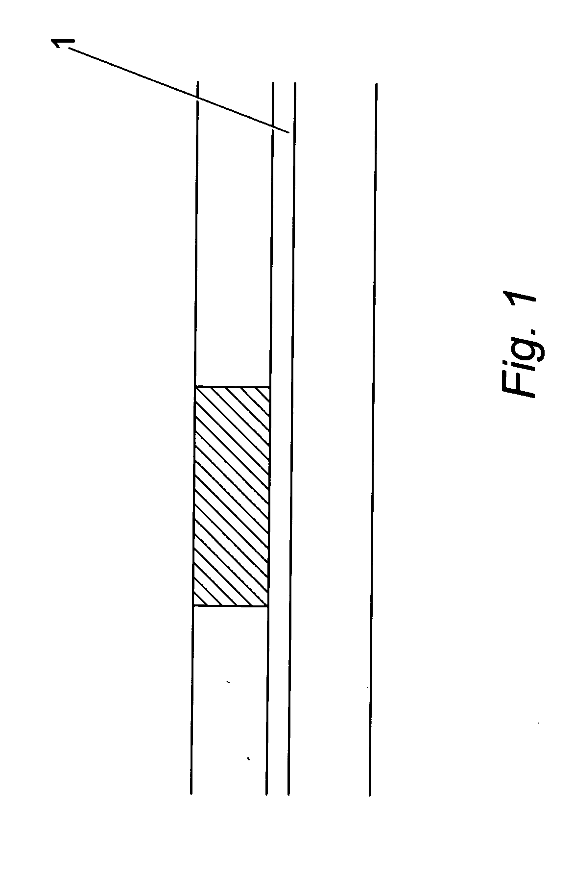
[0021]FIG. 1 is a cross-section of a typical prior art semiconductor construction;

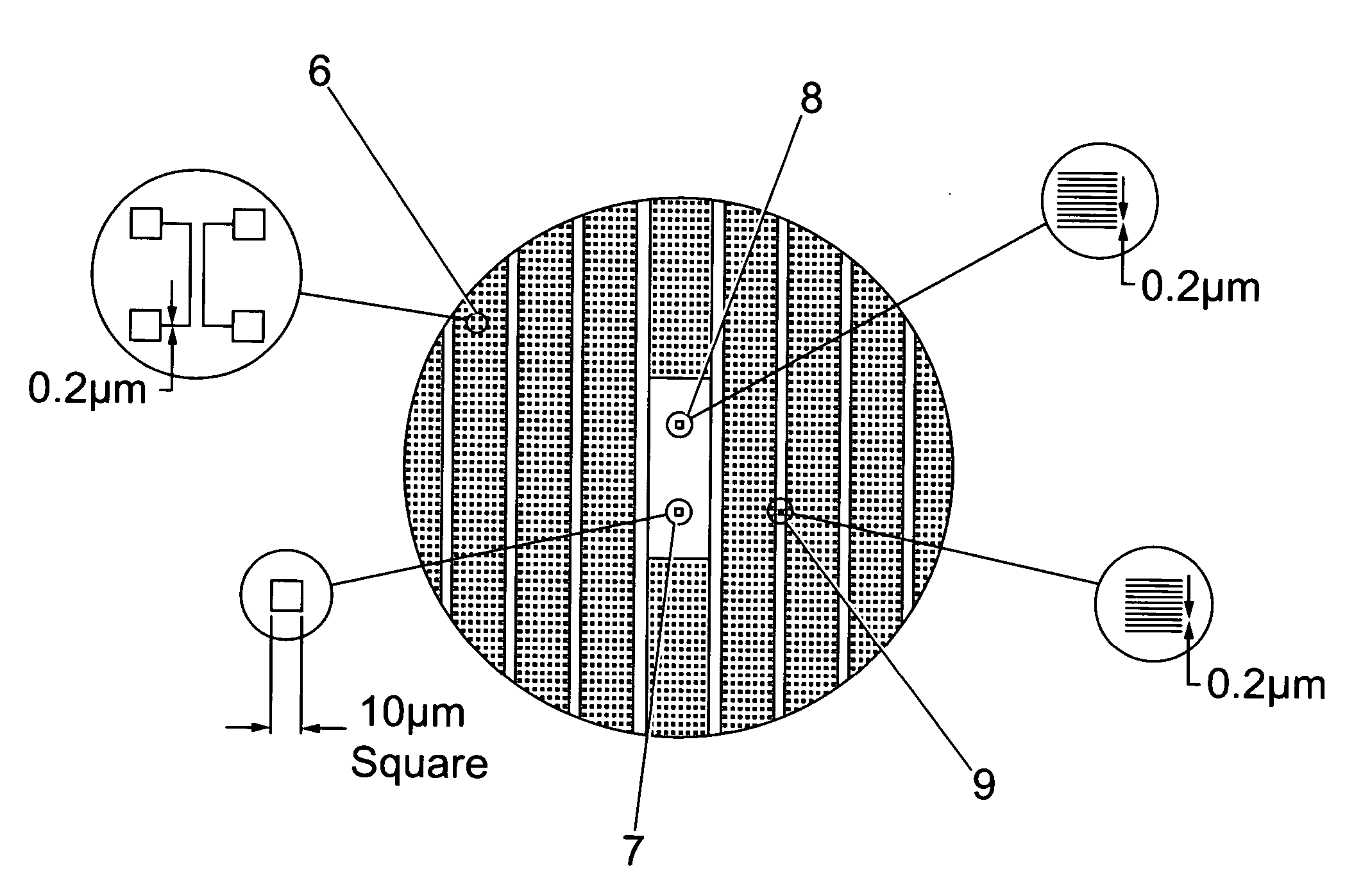
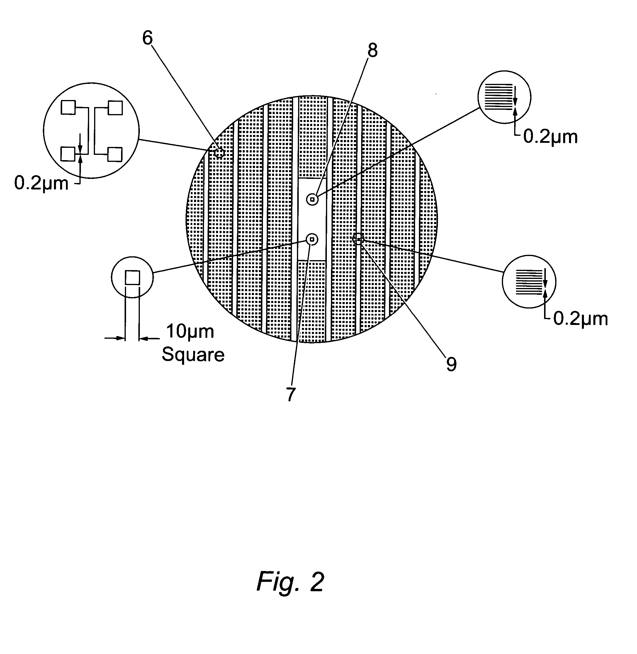
[0022]FIG. 2 is a front view of a silicon wafer showing structures used in the method of the invention;

[0023]FIG. 3 is a cross-section of part of FIG. 2 to an enlarged scale;

[0024]FIG. 4 is a schematic of an apparatus embodying the invention; and

[0025]FIG. 5 shows part of the apparatus of FIG. 4 in greater details.

[0026] A typical section of the etched dielectric for the semiconductor conductor deposition scheme known as ‘Damascene’ is shown in profile in FIG. 1. Typically the structure is etched down to an etch stop layer 1 which layer provides for a slowing down of the etch so that the etch may be terminated by reference to time or alternatively the distinguishing chemical composition of the etch stop layer 1 may be determined by reference to specific wavelengths of ligh...


PUM


Abstract

This invention relates to the control of etch and deposition processes in the manufacture of semiconductor devices, microelectronic machines (MEMs), and waveguides.

Description

FIELD OF THE INVENTION [0001] This invention relates to the control of etch and deposition processes in the manufacture of semiconductor devices, microelectronic machines (MEMs), and waveguides. BACKGROUND TO THE INVENTION [0002] It is well known that interferometric techniques can be applied to determining the endpoint in thin film deposition or etch. However, these techniques have been limited in their application to feature sizes of a few microns or greater, since the probe light is incapable of resolving smaller structures due to the diffraction limit of the probe light. Contemporary feature structures are becoming so small that they are less than the diffraction limit in dimension and the prior art techniques are becoming less useful and applicable because of this limit. [0003] An object of the present invention is accordingly to provide a method of monitoring semiconductor processes such as etch and deposition involving small feature sizes. Desirable and achievable outcomes of...

Claims


Application Information

Patent Timeline
IPC IPC(8): B81C99/00G01B11/06G01N21/21H01L21/00H01L21/3065H01L21/311H01L21/3213H01L21/66H01L21/768
CPCB81C99/004G01N21/21H01J37/32972H01L21/3065H01L22/26H01L21/32136H01L21/67253H01L21/76802H01L21/31116
Inventor BOGER, MICHAEL STEPHENHOLBROOK, MARKHEASON, DAVIDL'HOSTIS, FLORIANREEVE, DAVID
Owner BOC GRP INC
Why Eureka
Try Eureka