Fluxless assembly of chip size semiconductor packages

a technology of semiconductor packages and electrical assemblies, applied in semiconductor devices, semiconductor/solid-state device details, electrical apparatus, etc., can solve the problems of toxic, long-term adverse impact on the environment, and wide-spread use of solder alloys containing,

Inactive Publication Date: 2005-02-24
AGNG
View PDF15 Cites 100 Cited by
  • Summary
  • Abstract
  • Description
  • Claims
  • Application Information

AI Technical Summary

Problems solved by technology

Yet another drawback of the prior art package is the widespread use of solder alloys containing lead, primarily because of the relatively low melting temperature of lead and the relatively high strength of the joints formed thereof when solidified.
Lead is toxic and can have a significant, long-term adverse impact on the environment when electronic devices with solder joints containing lead are disposed of, e.g., in landfills.

Method used


Image

  • Fluxless assembly of chip size semiconductor packages
  • Fluxless assembly of chip size semiconductor packages
  • Fluxless assembly of chip size semiconductor packages

Examples


Embodiment Construction

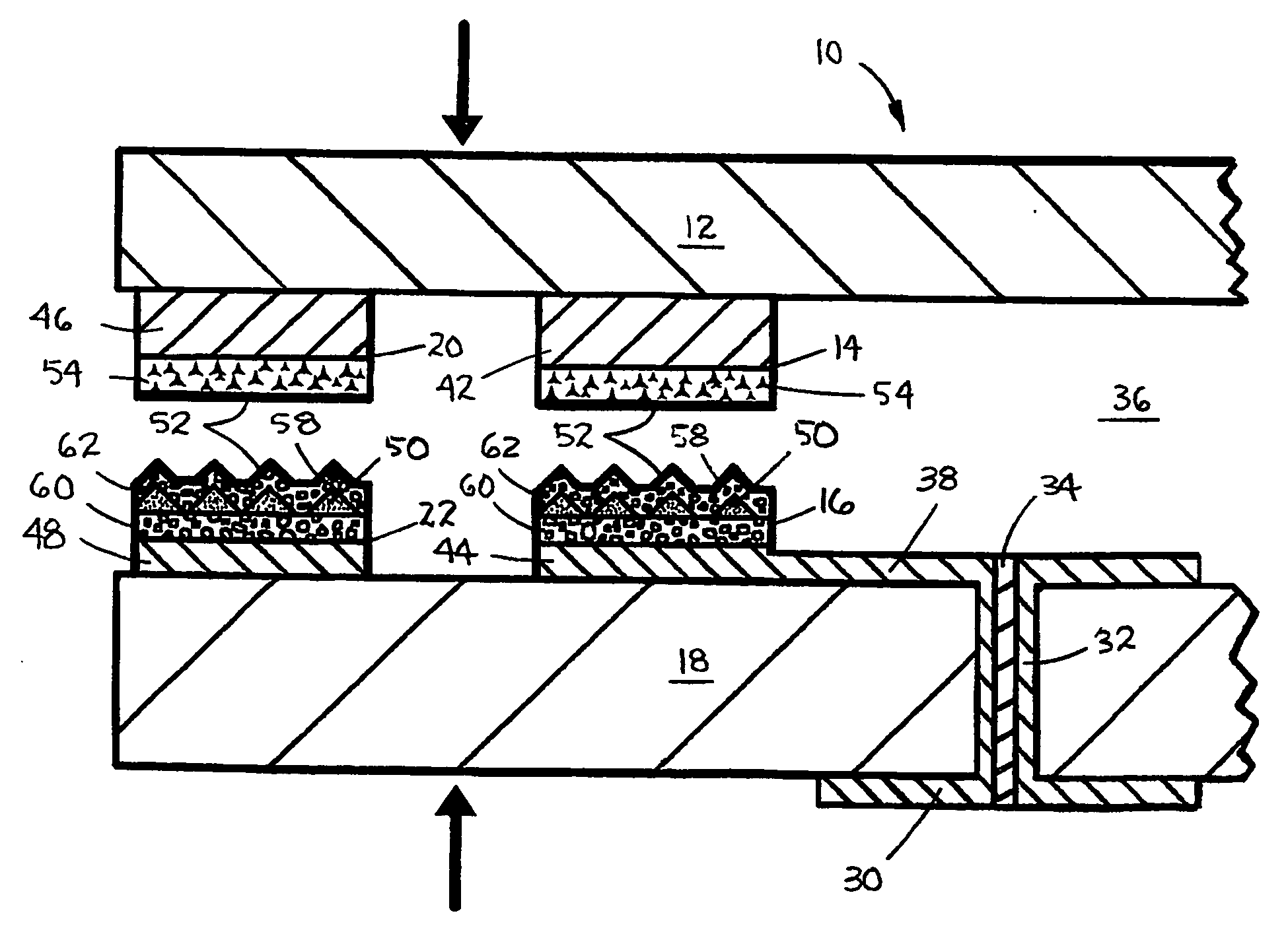
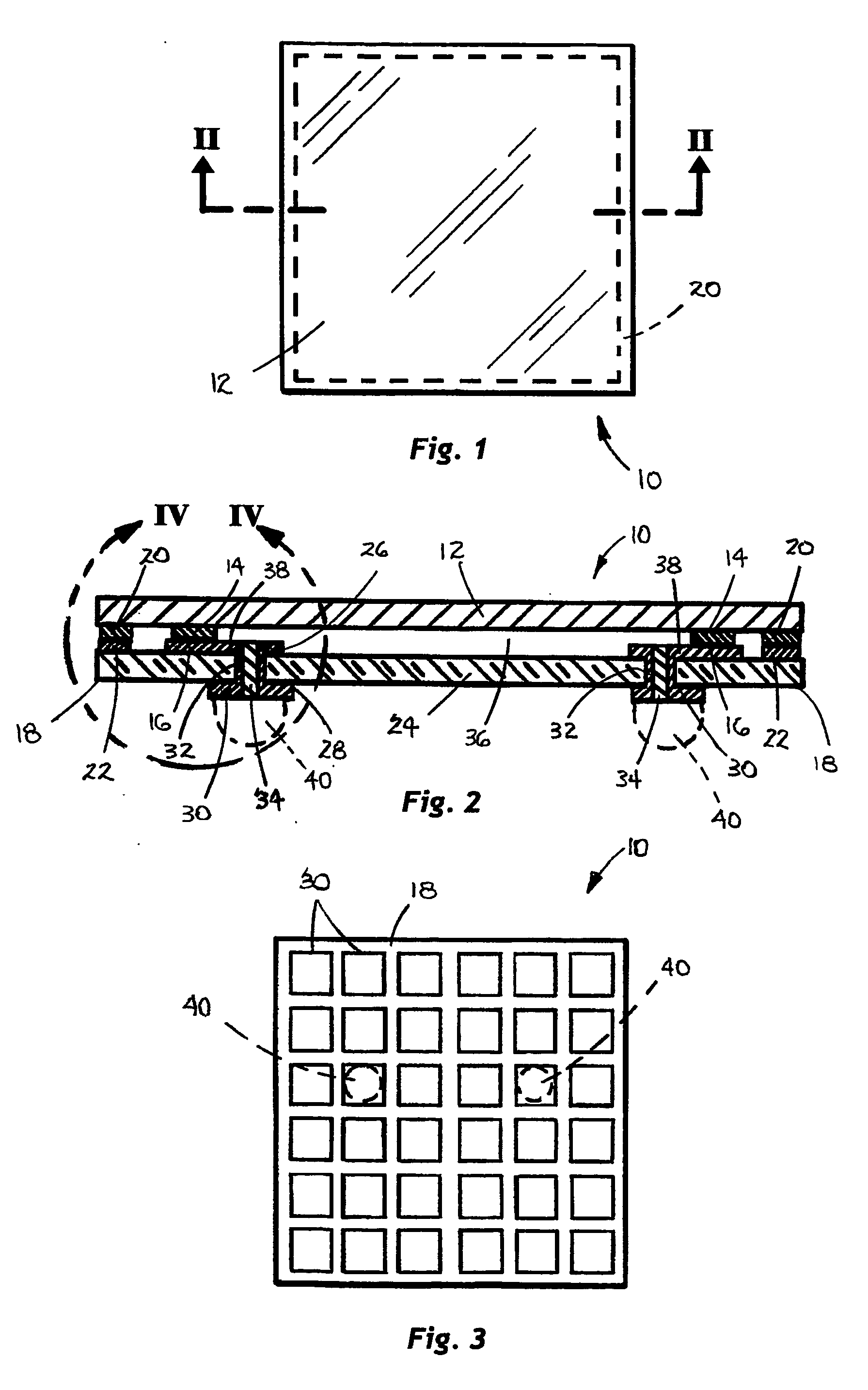
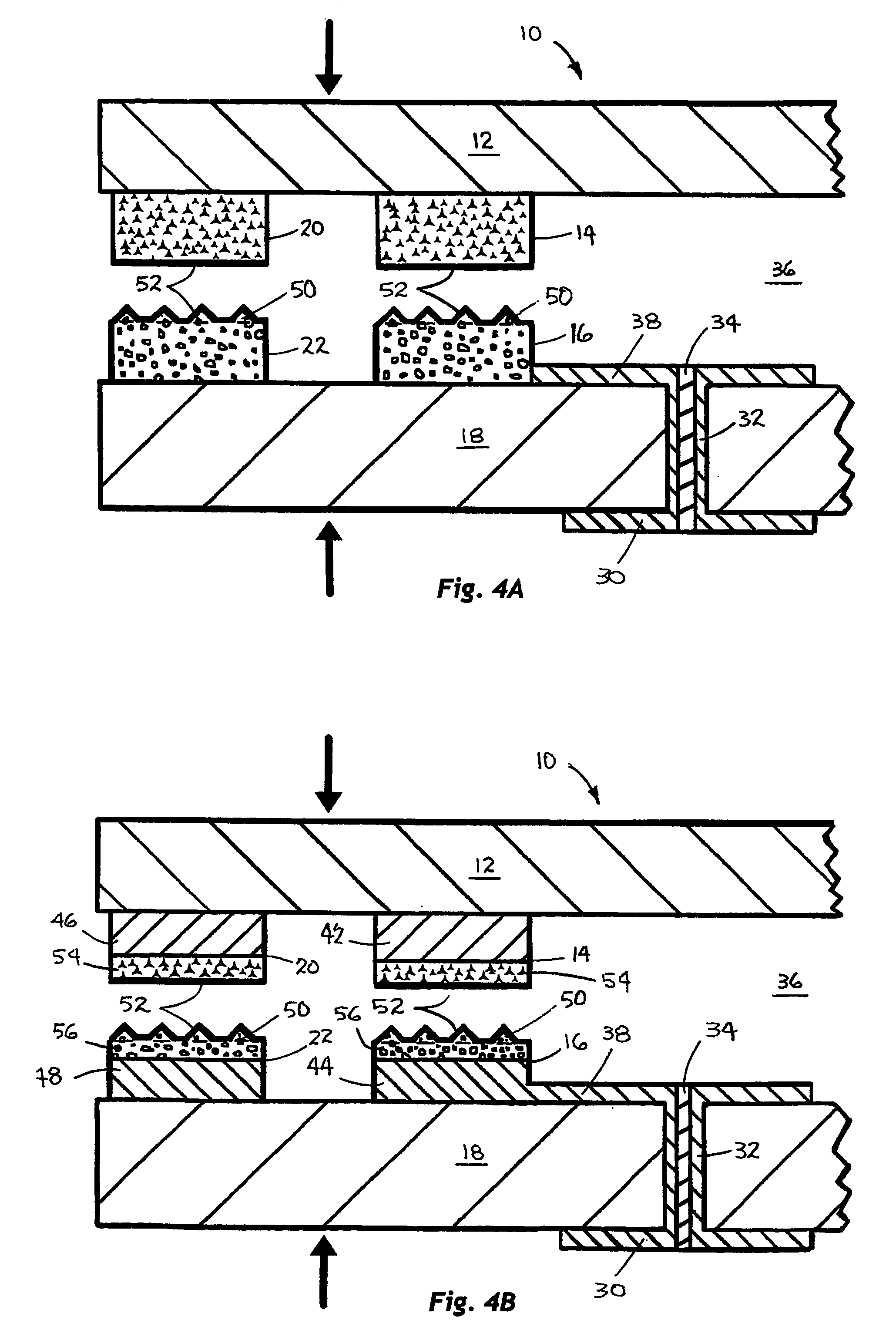
[0030] A chip size semiconductor package 10 assembled in accordance with the method of the present invention is illustrated in the top plan, cross-sectional elevation, and bottom plan views of FIGS. 1-3, respectively. The novel package 10 comprises a first substrate 12, e.g., a semiconductor die, having a first, active surface with one or more electrically conductive first pads 14, e.g., signal I / O pads, formed thereon, soldered to and in electrical connection with one or more corresponding electrically conductive second pads 16, e.g., signal connection pads, formed on a first surface of a second substrate 18, e.g., an interconnective substrate of the package 10, in accordance with the method of the invention. Optionally, the respective first and second pads 14 and 16 of the die 12 and interconnective substrate 18 may further comprise a pair of corresponding first and second sealing frames 20 and 22, each extending around a periphery of a respective one of the first surfaces of the ...


PUM


Abstract

A method for assembling semiconductor packages (10) includes forming corresponding pairs of conductive pads (14, 16, 20, 22) on respective surfaces of a die (12) and an interconnective substrate (18). Each pad in each pair includes an upper portion comprising at least one component of an electrically conductive eutectic alloy. Sharp, upstanding peaks (50, 58) are formed on at least one of the pads in each pair. The die and substrate are forcefully abutted and the pads heated until the sharp peaks penetrate through oxide films (52) on the respective opposing pads in each pair and contact the upper surface of the other pad therein, thereby initiating pad fusion. The pads are then cooled to solidify the molten portions thereof into an electrically conductive joint between each corresponding pair of pads and a hermetic seal around the periphery of the package.

Description

TECHNICAL FIELD [0001] This invention relates, in general, to the soldering of one substrate to another with electrically conductive eutectic alloys, and in particular, to the electrical assembly and hermetic sealing of chip size semiconductor packages without the use of fluxes or reducing atmospheres. BACKGROUND ART [0002] Integrated circuits (“ICs”) are formed in the “active” surface of a single die, or “chip,” cut from a semiconductor wafer containing an integral array of identical dies. The dies are relatively small and fragile, are susceptible to harmful environmental elements, particularly moisture, and during operation, can generate a relatively large amount of heat in a relatively small volume. Accordingly, ICs are typically assembled in affordable, yet robust, packages that protect them from the environment, enable them to be reliably mounted to and interconnected with, for example, a printed circuit board (“PCB”) populated with associated electronic components, and to effe...

Claims


Application Information

Patent Timeline
Patent Type & Authority Applications(United States)
IPC IPC(8): H01L23/485H01L23/498
CPCH01L23/49811H01L24/10H01L24/13H01L2224/13099H01L2224/16225H01L2924/01013H01L2924/01027H01L2924/01029H01L2924/0103H01L2924/01032H01L2924/01074H01L2924/01078H01L2924/01079H01L2924/01082H01L2924/01322H01L2924/14H01L2924/15311H01L2924/16152H01L2924/01006H01L2924/01033H01L2924/01047H01L2924/014H01L2924/00H01L24/05H01L24/16H01L24/81H01L2224/05001H01L2224/05023H01L2224/05124H01L2224/05624H01L2224/05639H01L2224/05644H01L2224/05647H01L2224/05655H01L2224/05684H01L2224/13H01L2224/13023H01L2924/12042H01L2924/00014H01L2224/13025
Inventor GARYAINOV, STANISLAV AGOTMAN, ALEXANDER SNOVIKOV, VLADIMIR V
Owner AGNG
Why Eureka
Try Eureka