Methods of reducing plasma-induced damage for advanced plasma CVD dielectrics

a dielectric and plasma technology, applied in the field of organosilicate layer depositing on the substrate, can solve the problems of many types and stages of devices that can experience plasma-induced damage (pid), device damage, and device damage, and achieve the effect of minimizing the damage of the substra

Inactive Publication Date: 2005-02-24
APPLIED MATERIALS INC
View PDF4 Cites 10 Cited by
  • Summary
  • Abstract
  • Description
  • Claims
  • Application Information

AI Technical Summary

Benefits of technology

[0008] Embodiments of the invention provide a method for depositing an organosilicate layer on a substrate such that plasma-induced damage to the substrate is minimized. In one embodiment, a method of depositing an organosilicate layer on a substrate includes reacting a gas mixture comprising an organosilicon compound in a processing chamber in the presence of RF power to deposit an organosilicate layer on a substrate disposed on a substrat

Problems solved by technology

However, one problem that has been encountered with plasma processing in integrated circuit fabrication is device damage that occurs as a result of exposure of a device to plasma conditions.
It is believed that a non-uniform plasma environment may result in electric field gradients that lead to device damage.
While the susceptibility or degree of device damage typically depends at least partially on the stage of device fabrication and the typ

Method used


Image

  • Methods of reducing plasma-induced damage for advanced plasma CVD dielectrics
  • Methods of reducing plasma-induced damage for advanced plasma CVD dielectrics
  • Methods of reducing plasma-induced damage for advanced plasma CVD dielectrics

Examples


example 1

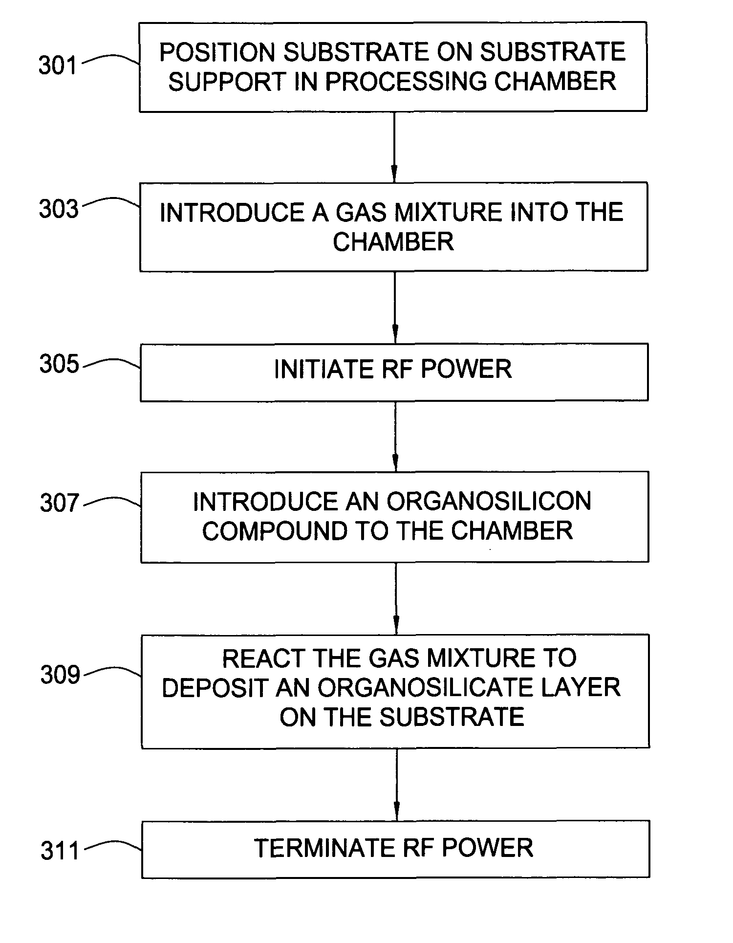
[0047] An organosilicate layer was deposited on a substrate from the following gas mixture at a chamber pressure of about 5.75 Torr and substrate temperature of 400° C.: [0048] Octamethylcyclotetrasiloxane (OMCTS), at about 520 sccm; [0049] Trimethylsilane (TMS), at about 300 sccm; [0050] Ethylene, at about 2,200 sccm; [0051] Oxygen, at about 1,000 sccm; and [0052] Helium, at about 1,000 sccm.

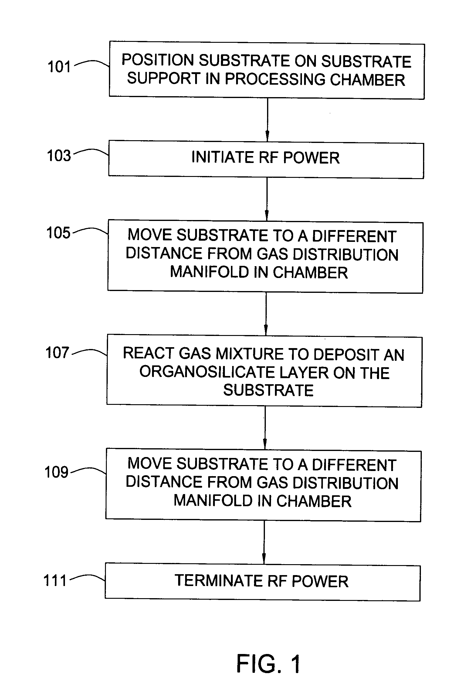
[0053] The substrate was positioned 300 mils from the gas distribution manifold, and RF power of 2.5 W / cm2 (800 W) at a frequency of 13.56 MHz was applied to the manifold. The gas mixture described above was introduced into the chamber before the initiation of RF power. After initiation of the RF power for about 2 seconds, the substrate was positioned 1050 mils from the gas distribution manifold for deposition of the organosilicate layer in about 20 seconds. The substrate was then positioned 700 mils from the gas distribution manifold, and the RF power was terminated in about 2 seconds, while ...

example 2

[0054] An organosilicate layer was deposited on a substrate from the following reactive gases at a chamber pressure of about 5.75 Torr and substrate temperature of 400° C.: [0055] Octamethylcyclotetrasiloxane (OMCTS), at about 520 sccm; [0056] Trimethylsilane (TMS), at about 300 sccm; [0057] Ethylene, at about 2,200 sccm; [0058] Oxygen, at about 1,000 sccm; and [0059] Helium, at about 1,000 sccm.

[0060] The substrate was positioned 1020 mils from the gas distribution manifold, and RF power of 2.5 W / cm2 (800 W) at a frequency of 13.56 MHz was applied to the manifold. The gas mixture described above was introduced into the chamber before the initiation of RF power. After initiation of the RF power for about 2 seconds, the organosilicate layer was deposited in about 20 seconds. The substrate was then positioned 700 mils from the gas distribution manifold, and the RF power was terminated in about 2 seconds. The chamber pressure was maintained at about 5.75 Torr and the gas mixture was r...

example 3

[0061] An organosilicate layer was deposited on a substrate from the following reactive gases at a chamber pressure of about 5.75 Torr and substrate temperature of 400° C.: [0062] Octamethylcyclotetrasiloxane (OMCTS), at about 520 sccm; [0063] Trimethylsilane (TMS), at about 300 sccm; [0064] Ethylene, at about 2,200 sccm; [0065] Oxygen, at about 1,000 sccm; and [0066] Helium, at about 1,000 sccm.

[0067] The substrate was positioned 1020 mils from the gas distribution manifold, and RF power of 2.5 W / cm2 (800 W) at a frequency of 13.56 MHz was applied to the manifold. The gas mixture described above was introduced into the chamber before the initiation of RF power. After initiation of the RF power for about 2 seconds, the organosilicate layer was deposited in about 20 seconds. The flow of the octamethylcyclotetrasiloxane and the trimethylsilane was terminated, and then the RF power was terminated in about 2 seconds while maintaining the chamber pressure. After the RF power was termina...


PUM

PropertyMeasurementUnit
Pressureaaaaaaaaaa
Poweraaaaaaaaaa
Flow rateaaaaaaaaaa

Abstract

A method for depositing an organosilicate layer on a substrate includes varying one or more processing conditions during a process sequence for depositing an organosilicate layer from a gas mixture comprising an organosilicon compound in the presence of RF power in a processing chamber. In one aspect, the distance between the substrate and a gas distribution manifold in the processing chamber is varied during processing. Preferably, the method of depositing an organosilicate layer minimizes plasma-induced damage to the substrate.

Description

BACKGROUND OF THE INVENTION [0001] 1. Field of the Invention [0002] Embodiments of the present invention generally relate to the fabrication of integrated circuits. More particularly, embodiments of the present invention relate to a method for depositing organosilicate layers on a substrate. [0003] 2. Description of the Related Art [0004] In the manufacture of integrated circuits, plasma processes are increasingly being used to replace thermal processes. Plasma processing provides several advantages over thermal processing. For example, plasma enhanced chemical vapor deposition (PECVD) allows deposition processes to be performed at substantially lower temperatures than the temperatures required for analogous thermal processes. This is advantageous for processes with stringent thermal budget demands, such as in very large scale or ultra-large scale integrated circuit (VLSI or ULSI) device fabrication. [0005] However, one problem that has been encountered with plasma processing in int...

Claims


Application Information

Patent Timeline
IPC IPC(8): C23C16/40C23C16/509H01L21/312H01L21/316H01L21/768
CPCC23C16/401C23C16/5096H01L21/02126H01L21/02216H01L21/76801H01L21/3122H01L21/31612H01L21/31633H01L21/02274
Inventor LI, LIHUATANAKA, TSUTOMUHUANG, TZU-FANGXIA, LI-QUNSUGIARTO, DIANSIVARAMAKRISHNAN, VISWESWARENLEE, PETER WAI-MANSILVETTI, MARIO DAVID
Owner APPLIED MATERIALS INC
Why Eureka
Try Eureka