Method to improve copper electrochemical deposition

a technology of electrochemical deposition and copper, which is applied in the field of electrochemical deposition methods and electrolyte solutions, can solve the problems of conformal nature of copper deposition, difficulty in filling increasingly high aspect ratio features, and difficulty in traditional deposition processes such as chemical vapor deposition (cvd), so as to reduce or avoid copper layer pitting and improve deposition uniformity

Inactive Publication Date: 2005-03-03
TAIWAN SEMICON MFG CO LTD
View PDF7 Cites 62 Cited by
  • Summary
  • Abstract
  • Description
  • Claims
  • Application Information

AI Technical Summary

Benefits of technology

[0012] To achieve the foregoing and other objects, and in accordance with the purposes of the present invention, as embodied and broadly described herein, the present invention provides a method for reducing or avoiding copper layer pitting in a copper electrochemical deposition process to improve deposition uniformity.

Problems solved by technology

Consequently, the aspect ratios for the features, i.e., their height divided by width, has increased thereby creating additional challenges in adequately filling the sub-micron features with, for example, copper metal.
Many traditional deposition processes such as chemical vapor deposition (CVD) have difficulty filling increasingly high aspect ratio features, for example, where the aspect ratio exceeds 2:1, and particularly where it exceeds 4:1.
Some problems that manifest themselves include the conformal nature of the copper deposition and the formation of keyholes and voids that occur when the top of the opening prematurely closes in the plating process.
Other problems have been associated with defects that occur at the end of the plating process where copper dendrites or protrusions may form on the copper surface from the electrolyte plating solution.
Despite various approaches proposed, nonuniformities in a copper plating process continue to manifest themselves, such as the formation of pits within the electroplated copper layer.

Method used


Image

  • Method to improve copper electrochemical deposition
  • Method to improve copper electrochemical deposition
  • Method to improve copper electrochemical deposition

Examples


Embodiment Construction

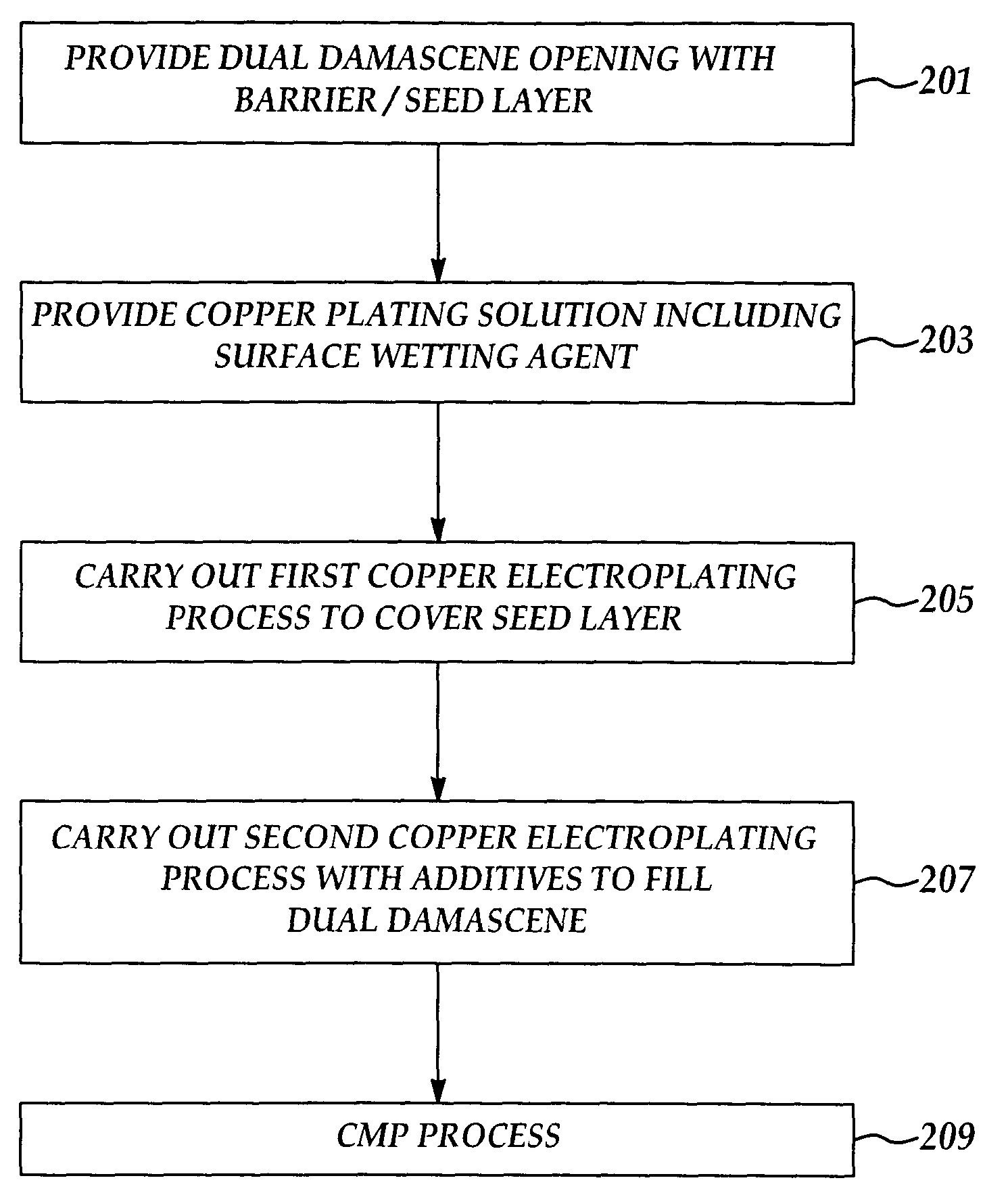
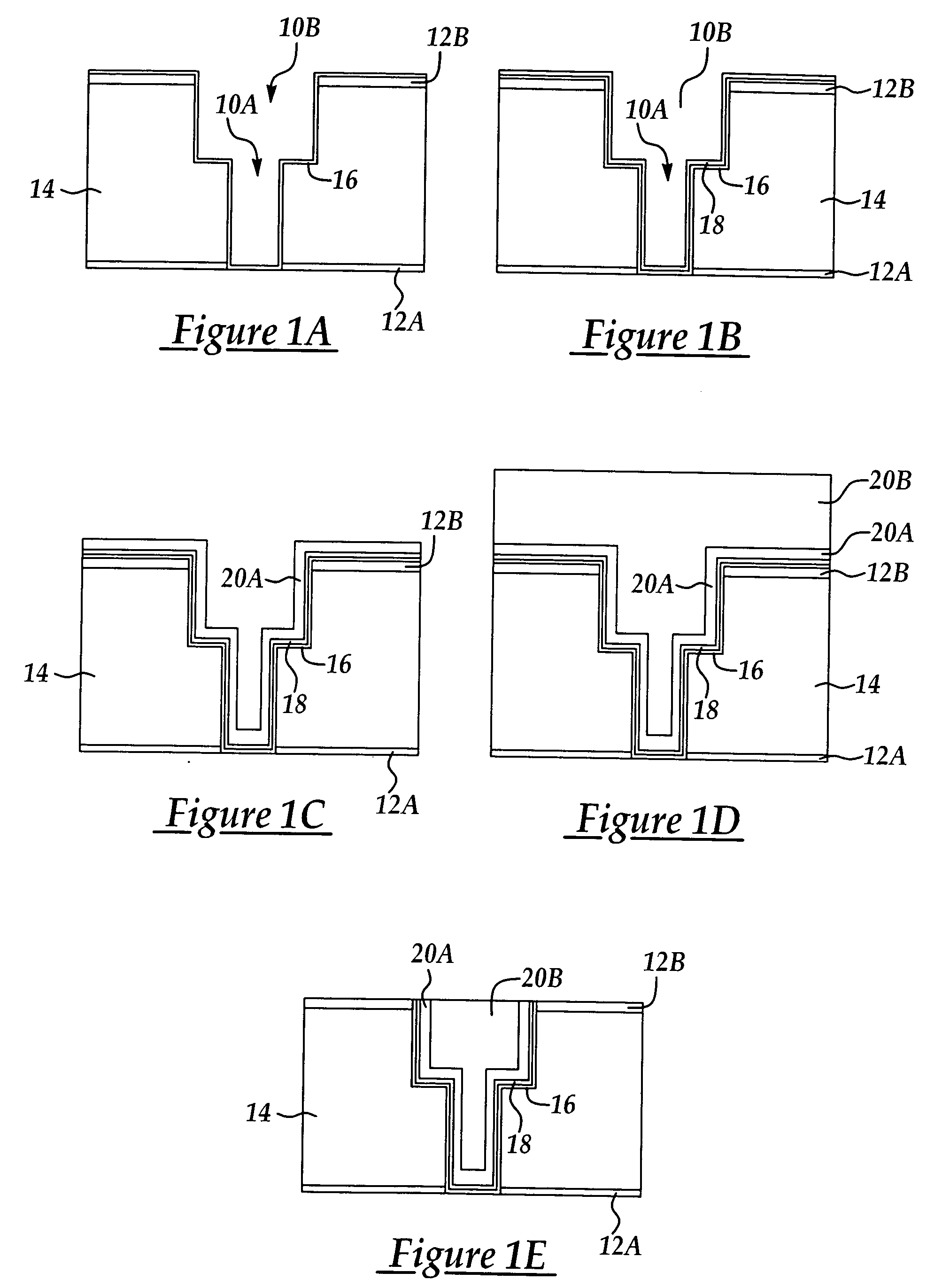
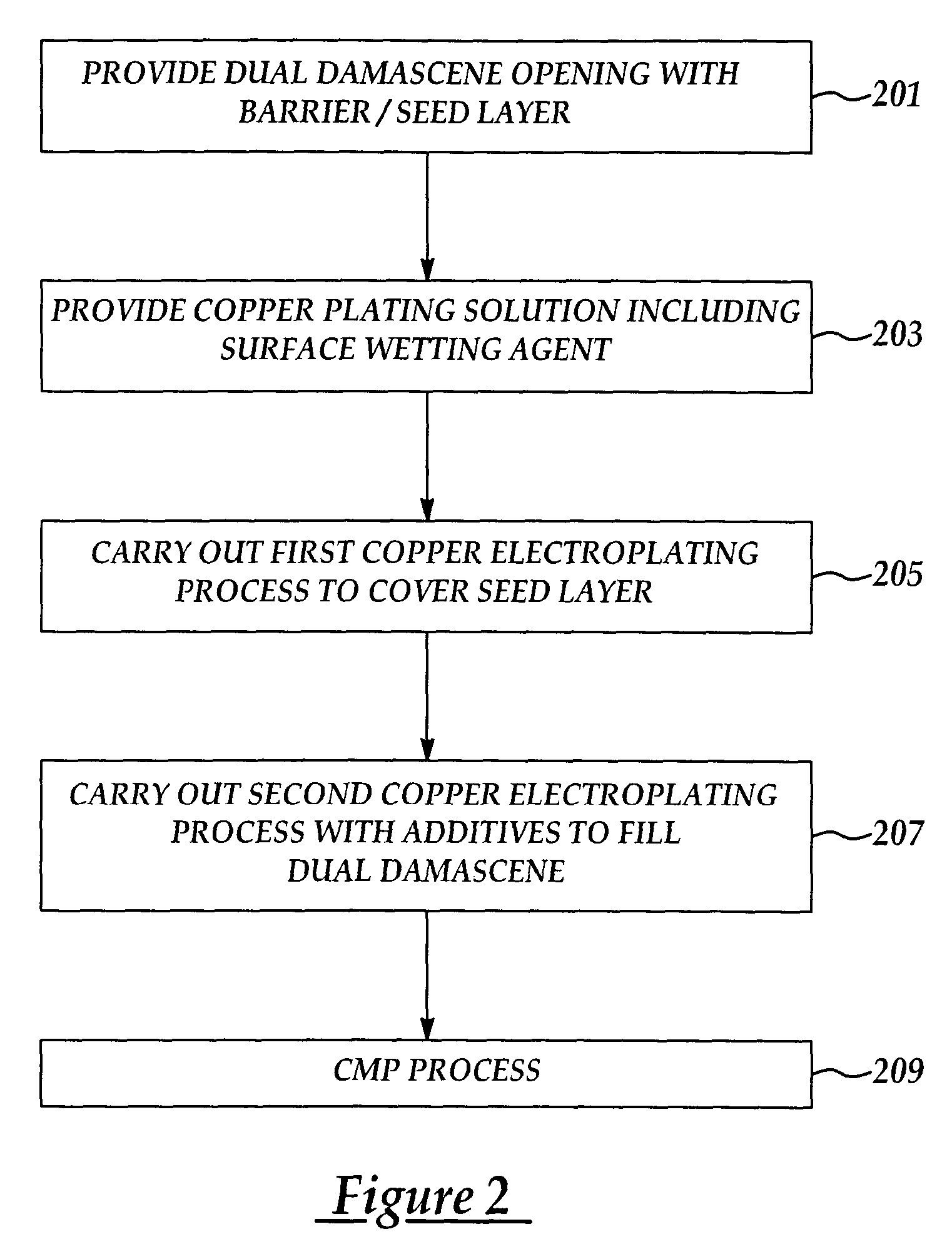
[0017] In the method and copper plating solution according to the present invention, the invention is explained by reference to electroplating of copper to fill a high aspect ratio opening, for example, a dual damascene structure. It will be appreciated, however, that the method of the present invention may be advantageously applied to the electroplating of single damascene structures as well as wide area trenches and bonding pads. It will be appreciated that the term copper as used herein refers to copper and alloys thereof.

[0018] In one embodiment of the invention, a copper plating solution is provided for carrying an electrochemical deposition (ECD) process on a substrate. The copper plating solution includes at least one soluble copper salt, an electrolyte, and a deforming (anti-forming) agent. The anti-forming agent is added at least prior to beginning the electroplating process to improve wetting of a copper seed layer to reduce generation of gaseous bubbles forming on the co...


PUM

PropertyMeasurementUnit
temperatureaaaaaaaaaa
diameteraaaaaaaaaa
aspect ratioaaaaaaaaaa

Abstract

A method for reducing or avoiding copper layer pitting in a copper electrochemical deposition process to improve deposition uniformity including providing a substrate for carrying out at least a first copper electroplating process; providing a copper electroplating solution including a deforming (antiforming) agent wherein the antiforming (deforming) agent includes at least one alkylene monomer; and, carrying out at least a first copper electroplating process to deposit at least a first copper layer.

Description

FIELD OF THE INVENTION [0001] This invention generally relates to electrochemical deposition (ECD) methods and electrolyte solutions and more particularly to methods for improving a copper plating solution to reduce plating solution bubble formation and improve copper ECD in a micro-integrated circuit manufacturing process. BACKGROUND OF THE INVENTION [0002] Sub-micron multi-level metallization is one of the key technologies for the next generation of ultra large scale integration (ULSI). The multilevel interconnects that lie at the heart of this technology require planarization of interconnect features formed in high aspect ratio apertures, including contacts, vias, metal interconnect lines and other features. Reliable formation of these interconnect features is very important to the success of ULSI and to the continued effort to increase circuit density and quality on individual substrates and die. [0003] Copper and copper alloys have become the metal of choice for filling sub-mic...

Claims


Application Information

Patent Timeline
Patent Type & Authority Applications(United States)
IPC IPC(8): C25D3/38C25D5/10C25D7/12C25D15/00H01L21/288H01L21/768H05K3/42
CPCC25D3/38C25D5/10C25D15/00C25D7/123H01L21/76877H05K3/423H01L21/2885
Inventor SHIH, CHIEN-HSUEHKO, TING-CHUTSAI, MINGHSING
Owner TAIWAN SEMICON MFG CO LTD
Why Eureka
Try Eureka