Semiconductor device

a technology of semiconductor devices and semiconductors, applied in semiconductor devices, semiconductor/solid-state device details, electrical apparatus, etc., can solve the problems of reduced reliability of semiconductor devices and difficulty in obtaining sufficient adhesiveness, and achieve the effect of reducing the size of the semiconductor devi

Active Publication Date: 2005-03-03
RENESAS ELECTRONICS CORP +1
View PDF7 Cites 19 Cited by
  • Summary
  • Abstract
  • Description
  • Claims
  • Application Information

AI Technical Summary

Benefits of technology

[0014] By the electroless plating of the wirings on the wiring board, the power supply wirings become unnecessary. Therefore, it is possible to form the wirings only at the inner sides of the bonding electrodes. In other words, it is no longer necessary to form the insulating film at the ou

Problems solved by technology

As a result, it is difficult to obtain sufficient adhesiveness and moisture-resistance of

Method used


Image

  • Semiconductor device
  • Semiconductor device
  • Semiconductor device

Examples


first embodiment

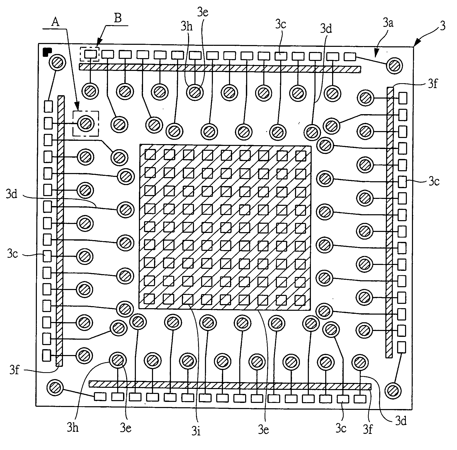
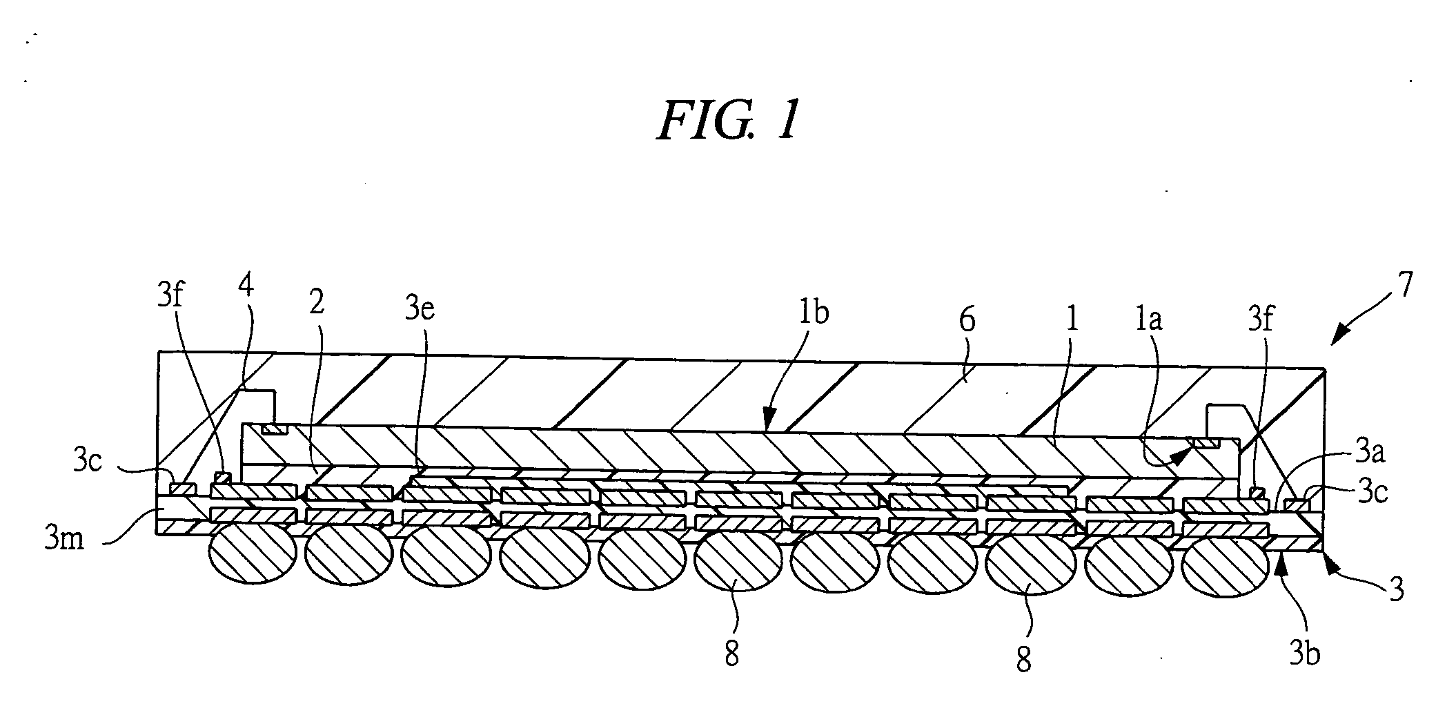
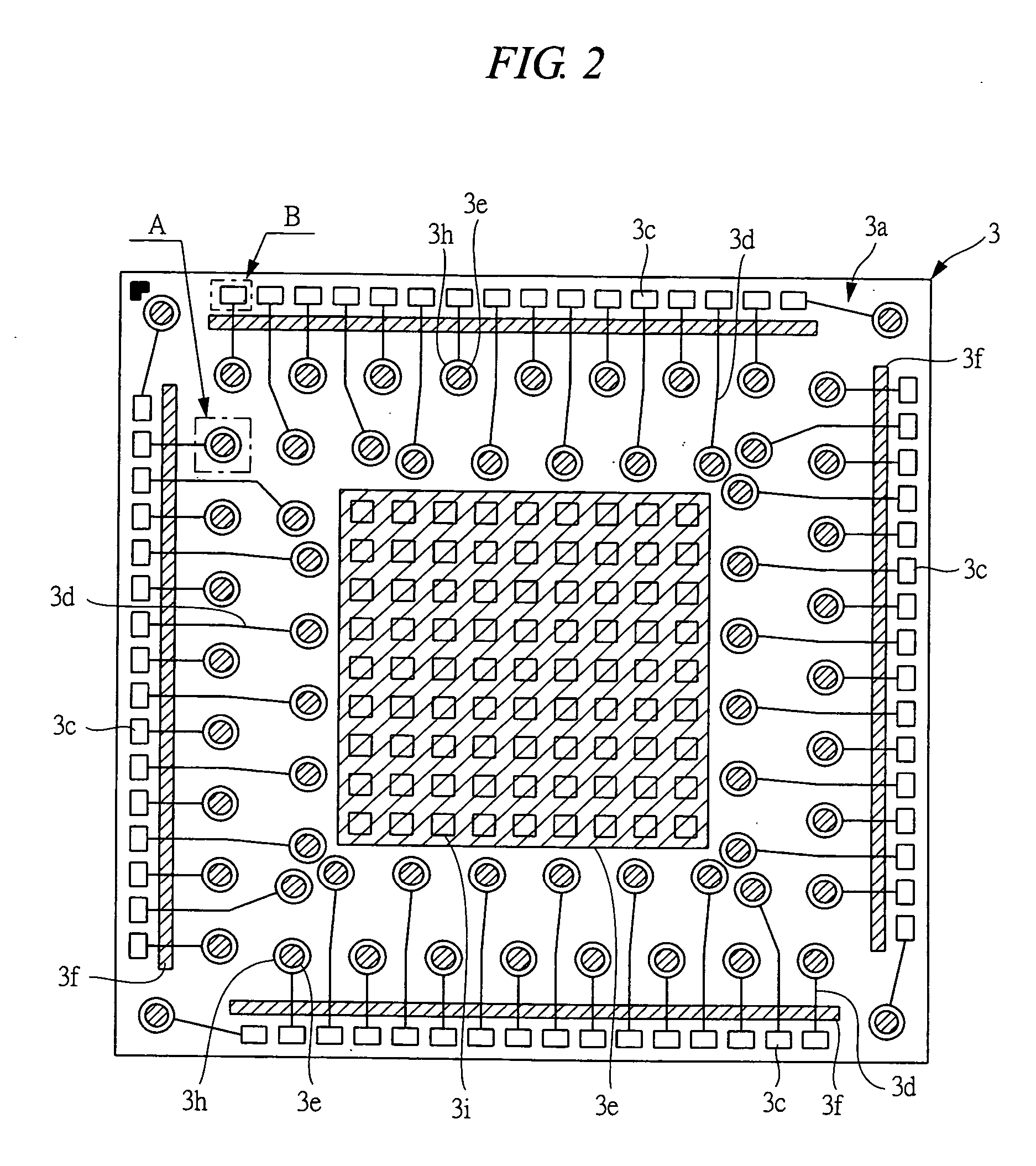
[0041] (First Embodiment)

[0042]FIG. 1 is a cross sectional view showing an example of the structure of a semiconductor device according to the first embodiment of the present invention, FIG. 2 is a plan view showing an example of the conductor pattern on the main surface of the wiring board incorporated in the semiconductor device of FIG. 1, FIG. 3 is a bottom plan view showing an example of the conductor pattern on the rear surface of the wiring board of FIG. 2, FIG. 4 is an enlarged partial plan view showing an example of the configuration of an area A in FIG. 2, FIG. 5 is an enlarged partial plan view showing a modified example of the configuration of the area A in FIG. 2, FIG. 6 is a plan view showing the insulating film formed on the main surface of the wiring board in a modified example, FIG. 7 is an enlarged partial plan view showing an example of the shape of the conductor pattern of an area B in FIG. 2, FIG. 8 is an enlarged partial plan view showing a modified example of t...

second embodiment

[0082] (Second Embodiment)

[0083]FIG. 13 is a plan view showing an example of the conductor pattern on the main surface of the wiring board according to the second embodiment of the present invention, FIG. 14 is a bottom plan view showing the conductor pattern on the rear surface of the wiring board of FIG. 13, FIG. 15 is a plan view showing the conductor pattern on the main surface of the wiring board in a modified example of the second embodiment of the present invention, FIG. 16 is a bottom plan view showing the conductor pattern on the rear surface of the wiring board of FIG. 15, FIG. 17 is a plan view showing the conductor pattern on the main surface of the wiring board in a modified example of the second embodiment of the present invention, FIG. 18 is a bottom plan view showing the conductor pattern on the rear surface of the wiring board of FIG. 17, FIG. 19 is a plan view showing the conductor pattern on the main surface of the wiring board in a modified example of the second ...


PUM


Abstract

A semiconductor device comprises: a package substrate having a plurality of bonding electrodes arranged in a peripheral region of a main surface thereof and wirings connected to the respective bonding electrodes and electrolessly plated; a semiconductor chip mounted on the package substrate; a plurality of wires connecting pads of the semiconductor chip and the bonding electrodes; a sealing body for sealing the semiconductor chip and the wires with resin; and a plurality of solder balls arranged on the package substrate. The wirings are formed only at the inner side of the plurality of bonding electrodes on the main surface of the package substrate, and no solder resist film is formed at the outer side of the plurality of bonding electrodes. With this arrangement, the region outside the bonding electrodes can be minimized and the semiconductor device can be downsized without changing the size of the chip mounted thereon.

Description

CROSS-REFERENCE TO RELATED APPLICATION [0001] The present application claims priority from Japanese Patent Application JP 2003-303858 filed on August. 28, 2003, the content of which is hereby incorporated by reference into this application. TECHNICAL FIELD OF THE INVENTION [0002] The present invention relates to a semiconductor device and, more particularly, it relates to a technique that can be effectively applied to a semiconductor device comprising a wiring board and a semiconductor chip mounted thereon. BACKGROUND OF THE INVENTION [0003] A conventional semiconductor package (semiconductor device) having a substrate for mounting a semiconductor element (wiring board) is manufactured by laminating a photosensitive coverlay film with a thickness of 30 μm to be an insulating coating (insulating film) on the connection land side of the substrate, opening external connection terminals by development, and electrolessly plating the surface of the wiring conductor sequentially with nicke...

Claims


Application Information

Patent Timeline
IPC IPC(8): H01L23/02H01L23/12H01L23/498
CPCH01L23/49838H01L2224/48227H01L2224/45144H01L24/49H01L24/48H01L2924/15311H01L2224/49175H01L2924/01046H01L2924/01078H01L2924/01079H01L2924/00H01L2924/00014H01L24/45H01L2924/181H01L2224/05599H01L2924/00012H01L23/02H01L23/12
Inventor TAKAHASHI, NORIYUKIICHITANI, MASAHIROICHITANI, RUMIKO
Owner RENESAS ELECTRONICS CORP
Why Eureka
Try Eureka