Flip-chip interconnect with increased current-carrying capability

a chip and current-carrying technology, applied in the field of circuit devices, can solve the problems of “electrically open” solder joints, general unsolderability and corrosion of aluminum and its alloys, and achieve the effect of improving the current-carrying capability of solder bump connections

Inactive Publication Date: 2005-03-03
DELPHI TECH INC
View PDF8 Cites 0 Cited by
  • Summary
  • Abstract
  • Description
  • Claims
  • Application Information

AI Technical Summary

Benefits of technology

[0011] The present invention is directed to improving the current-carrying capability of solder bump connections between metal layers on a surface-mount circuit device and a substrate to which the device is attached with the connections. The present invention employs a metal layer comprising at least one leg portion and a pad portion, with the pad portion having a continuous region and a plurality of separate electrical paths leading to and from the continuous region. The electrical paths are delineated in the pad portion by nonconductive regions, such as openings defined in the pad portion, with at least some of the openings preferably extending into the leg portion.
[0012] The metal layer of this invention is adapted to carry current to and from a solder bump electrically connected to the continuous region. The multiple electrical paths split the current flow to and from the solder bump, and distribute the current around the perimeter of the solder bump in a manner that reduces current density in regions of the solder bump where current would otherwise be concentrated. While current density can also be reduced by increasing the thickness of the metal, the present invention achieves reduced current densities without the cost of the additional metal required to increase the thickness of the metal layer. The multiple electrical paths of the metal layer can be defined in the metal layer during conventional processes undertaken to pattern the metal layer on the device surface.

Problems solved by technology

Aluminum and its alloys are generally unsolderable and susceptible to corrosion if left exposed, and copper is readily dissolved by molten solder.
This segregation is detrimental to the long term reliability and performance of the solder bump connection, and in some cases can lead to “electrically open” solder joints.
Flip chip solder connections used in high power applications, such as output drivers for automotive engine controllers, are particularly likely to exhibit excessive resistances and open connections associated with electromigration.

Method used


Image

  • Flip-chip interconnect with increased current-carrying capability
  • Flip-chip interconnect with increased current-carrying capability
  • Flip-chip interconnect with increased current-carrying capability

Examples


Embodiment Construction

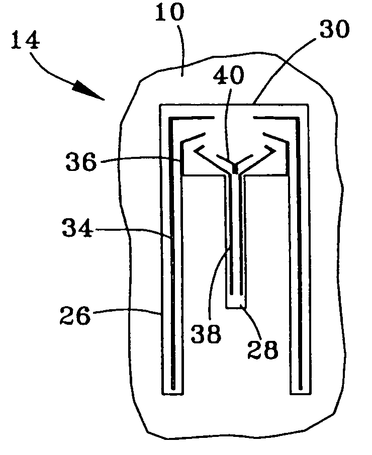
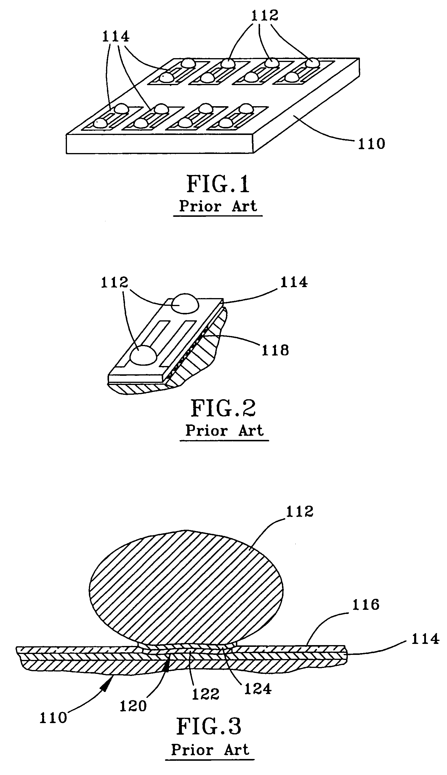
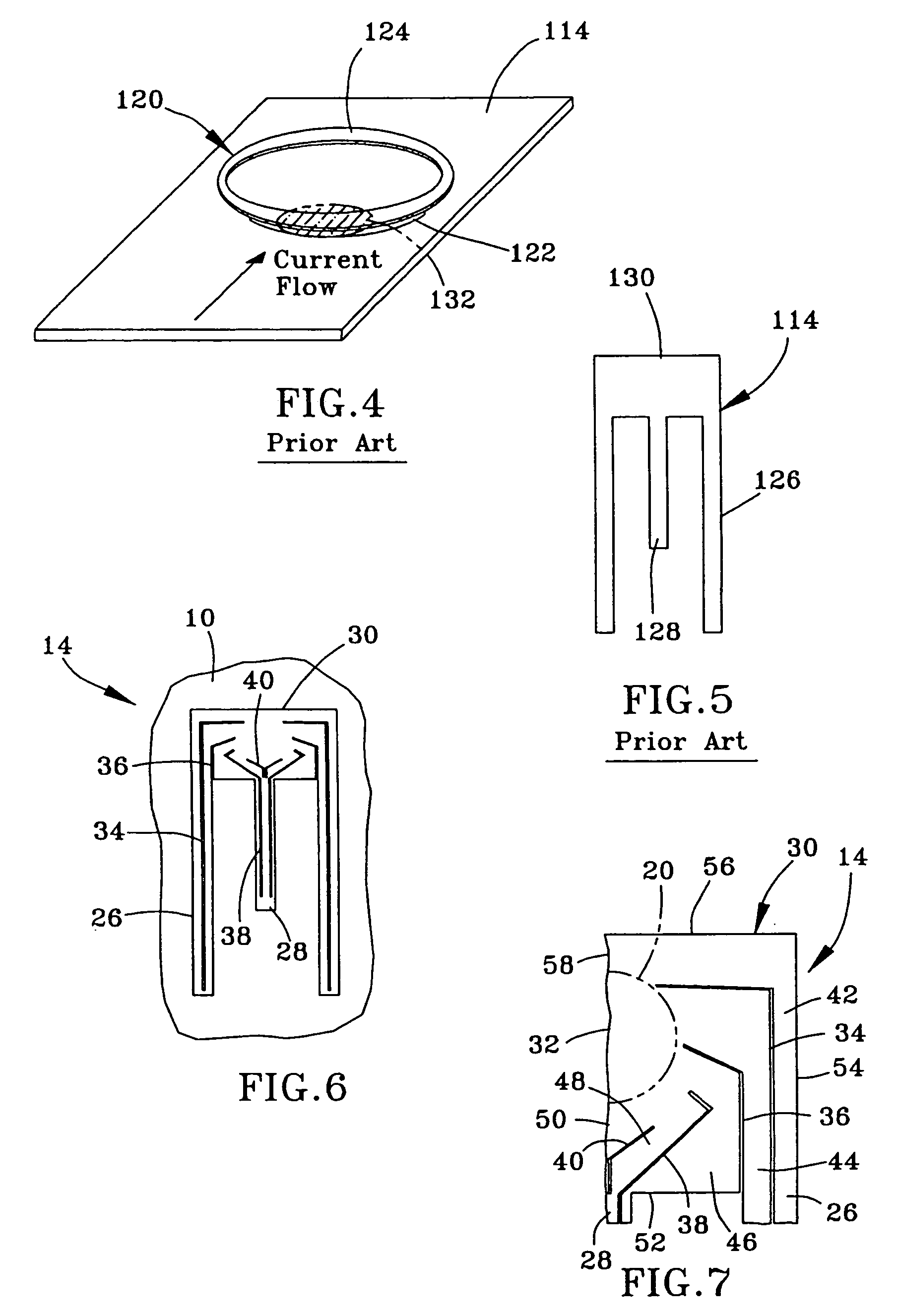
[0021] The present invention is directed to improving the reliability of surface-mount devices, such as flip chips of the type represented in FIGS. 1 through 3. According to one aspect of the present invention, current density within a solder bump (e.g., 112 in FIGS. 1 through 3) significantly contributes to electromigration, and therefore controlling current density can be effective in minimizing and preventing open solder connections caused by electromigration. Current density in a structure is defined as current flow per unit area (in a plane perpendicular to the direction of current flow) at various points in a structure, and is a good indicator of least resistant paths for electrical current flow through the structure.

[0022] In an investigation leading to this invention, it was observed that portions of a solder bump that have considerably higher current density than the bulk of the solder bump are more prone to electromigration. A solder bump inherently poses some level of re...


PUM


Abstract

A metal runner that improves the current-carrying capability of solder bumps used to electrically connect a surface-mount circuit device to a substrate. The runner comprises at least one leg portion and a pad portion, with the pad portion having a continuous region and a plurality of separate electrical paths leading to and from the continuous region. The electrical paths are delineated in the pad portion by nonconductive regions defined in the pad portion, with at least some of the nonconductive regions extending into the leg portion. The multiple electrical paths split the current flow to and from the solder bump, distributing the current around the perimeter of the solder bump in a manner that reduces current density in regions of the solder bump where electromigration is most likely.

Description

CROSS REFERENCE TO RELATED APPLICATIONS [0001] Not applicable. STATEMENT REGARDING FEDERALLY SPONSORED RESEARCH [0002] Not applicable. BACKGROUND OF THE INVENTION [0003] (1) Field of the Invention [0004] The present invention generally relates to circuit devices of the type that are attached to a substrate with multiple solder connections. More particularly, this invention relates to conductive layers on such a device, wherein the conductive layers are configured to promote the current-carrying capability of the solder connections of the device. [0005] (2) Description of the Related Art [0006] Surface-mount (SM) semiconductor devices such as flip chips and ball grid arrays (BGA's) are attached to substrates with beadlike terminals formed on interconnect pads located on one surface of the device. The terminals are usually in the form of solder bumps that, after placement of the chip on the substrate, are reflowed to both secure the chip to the substrate and electrically interconnect ...

Claims


Application Information

Patent Timeline
Patent Type & Authority Applications(United States)
IPC IPC(8): H01L23/485H01L23/528
CPCH01L23/528H01L24/02H01L24/10H01L2224/0401H01L2924/01013H01L2924/14H01L2924/01033H01L2924/0105H01L2924/01082H01L2924/01322H01L2924/014H01L2924/01029H01L2224/02375H01L24/05H01L24/13H01L2224/05548
Inventor MITHAL, PANKAJHIGDON, WILLIAM D.GOSE, MARK W.DIKEMAN, JOHN M.STEPNIAK, FRANK
Owner DELPHI TECH INC
Why Eureka
Try Eureka