High electron mobility transistor with multiple channels

a high electron mobility, transistor technology, applied in the direction of basic electric elements, electrical equipment, semiconductor devices, etc., can solve the problems of controllability issues or lattice damage problems, depleting the 2deg underneath the gate region, and slowed down the electrons, so as to achieve enhanced current carrying capability, high electron mobility transistors, and preservation of current carrying capability

Active Publication Date: 2014-12-09
MITSUBISHI ELECTRIC RES LAB INC
View PDF24 Cites 6 Cited by
  • Summary
  • Abstract
  • Description
  • Claims
  • Application Information

AI Technical Summary

Benefits of technology

[0012]An objective of present invention is to provide a device, such as a high electron mobility transistor (HEMT) having enhanced current carrying capability. It is a further objective of some embodiments to provide a HEMT device having multiple-channel conduction paths. It is a further objective of some embodiments to provide a HEMT operative at low voltage while preserving current carrying capability. It is a further objective of some embodiments to provide a HEMT with both symmetrical and asymmetrical gate control and with flexible channel conduction path development. It is a further objective of some embodiments to provide a HEMT with either E-mode / D-mode or mixed E-mode and D-mode operation.
[0013]Some embodiments of the invention are based on a realization that that different polarity nitride stacks can be used to create a HEMT having multiple channels forming at least part of the conduction path between the source and the drain. Specifically, if the stacks of the HEMT have different polarity, then the interference between the channels is minimized, as contrasted with interference of the channels form by stacks of the same polarity.
[0015]It is further recognized that it is advantageous to carefully select the thickness of the gate dielectric material and thickness. This is because that the properties of gate dielectric layer are in relation to the gate voltage on the control of capacitive coupling between gate and GaN layer. For example, in some embodiments, the equivalent oxide thickness of the surface gate dielectric layers is inversely proportional to the metal-insulator-oxide capacitance. A careful selection should ensure that a minimum voltage is sufficient to control the 2DEG channel and to create and control the inversion carrier channel.
[0016]Some embodiments take advantage of minimizing the thickness of the layers of the stack till optimum thickness avoiding interference between the dual channels. This can be performed for both double-gate and single-gate multiple channel devices.
[0017]It is further recognized that the flexibility of the gate control can develop multiple channels. This is because the channel generation is a function of voltage applied to the gate. In some embodiments of the invention with double gate structure, by applying symmetrical or asymmetrical gate control, a variety number of channels can be induced at different gate biases. In some embodiments of the invention with single gate structure, by applying gate control at different voltages, a variety number of channels can be developed.

Problems solved by technology

However, those electrons are slowed down by collisions with the impurities (dopants) used to generate the electrons.
Those techniques can deplete the 2DEG underneath the gate region but suffer from either controllability issue or lattice damage problems.
However, despite the increased performance of the N-polar devices, the drive current under low voltage bias for N-polar GaN HEMT is smaller than the state-of-the-art Ga-polar GaN HEMT.
This limitation of the drive current degrades the RF amplification capability and limits the output power density of the device.
A depletion-mode single gate double channels Ga-polar GaN HEMT, described by Rongming Chu, “AlGaN—GaN Double-Channel HEMTs,” IEEE Transactions on Electron Device Letters, Vol. 52, No. 4, Page 438, April 2005, generates channel in each GaN layer but lacks of gate control on both channels and is not suitable for power failure protection application.

Method used


Image

  • High electron mobility transistor with multiple channels
  • High electron mobility transistor with multiple channels
  • High electron mobility transistor with multiple channels

Examples


Embodiment Construction

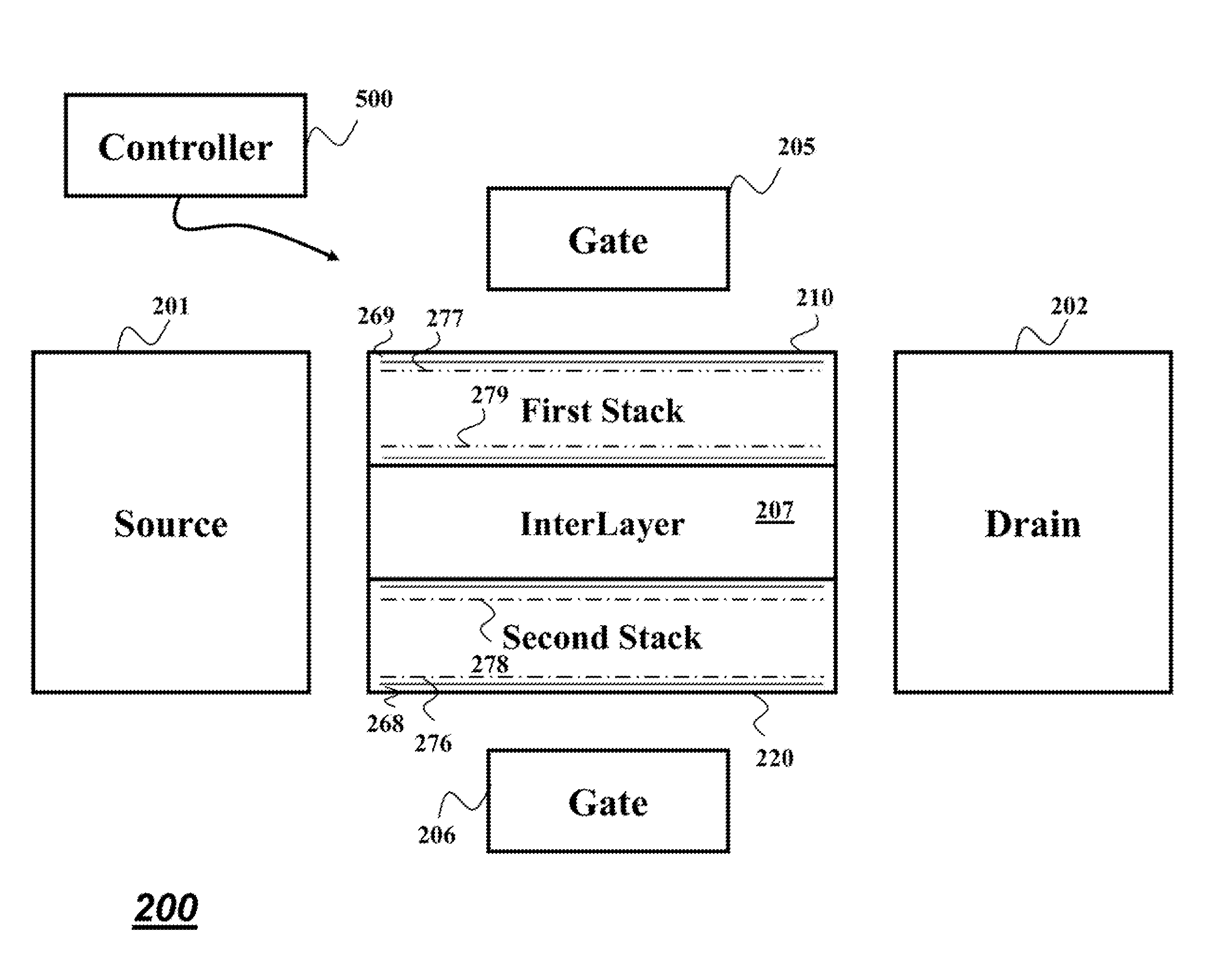
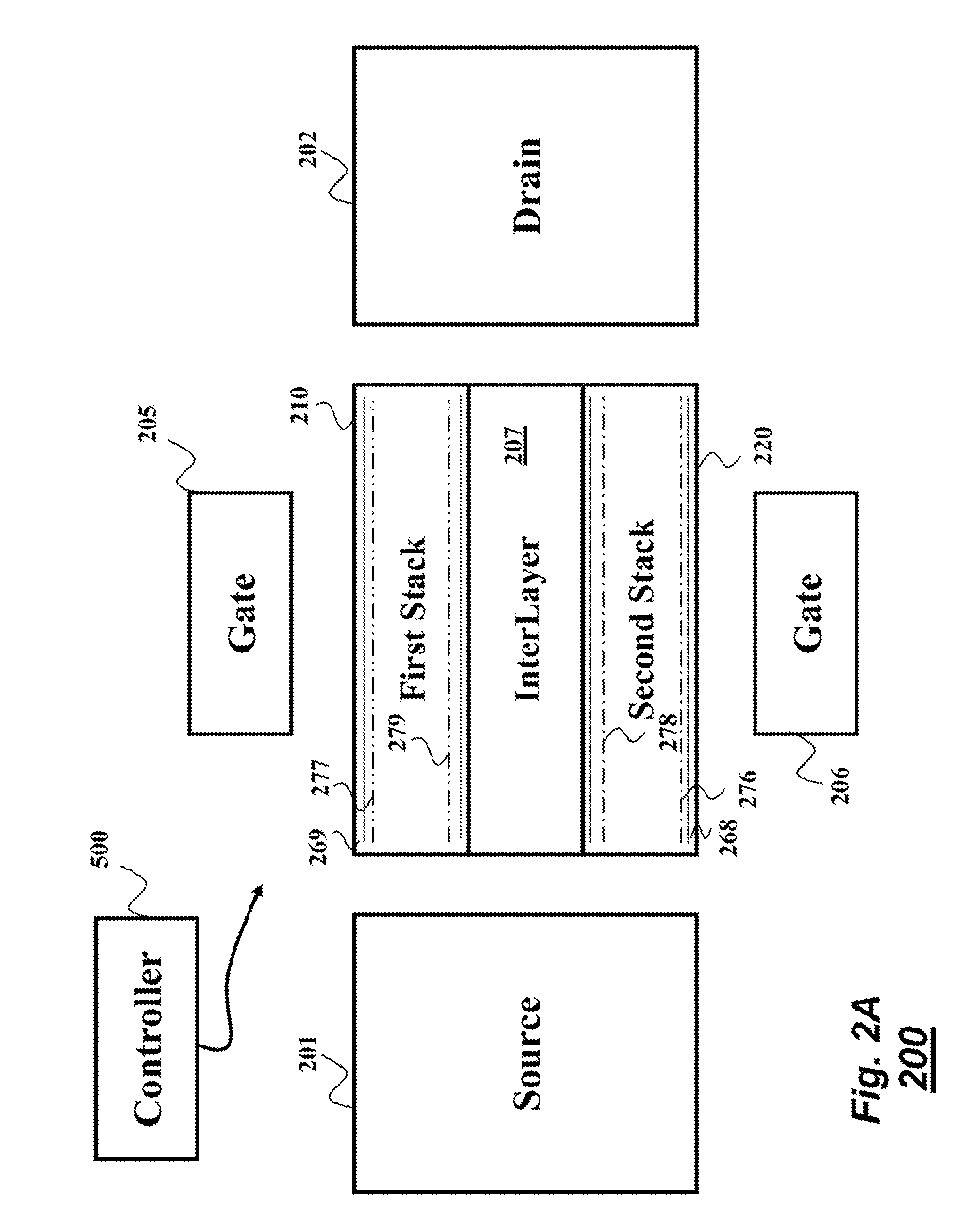
[0044]FIG. 2A shows a schematic of a device 200 designed according to some embodiments of the invention. The device can be a high electron mobility transistor (HEMT) including a source 201 for transmitting electronic carriers, and a drain 202 for receiving electronic carriers. The device also includes two stacks of different polarity for providing at least part of a conduction path between the source and the drain, i.e., a first stack 210 and a second stack 220. The device can also include a interlayer 207 deposited between the first and the second stacks, and at least one gate 205 operatively connected to at least the first stack for controlling a conduction of the electronic charge.

[0045]In various embodiments, the first and the second stack are heterostructures including a gallium nitride (GaN) layer for generating two-dimensional electron gas (2DEG) channels due to polarization difference at heterojunction. For example, the gate 205 controls the conduction of the electronic char...


PUM


Abstract

A device includes a source and a drain for transmitting and receiving an electronic charge. The device also includes a first stack and a second stack for providing at least part of a conduction path between the source and the drain, wherein the first stack includes a first gallium nitride (GaN) layer of a first polarity, and the second stack includes a second gallium nitride (GaN) layer of the second polarity, and wherein the first polarity is different from the second polarity. At least one gate operatively connected to at least the first stack for controlling a conduction of the electronic charge, such that, during an operation of the device, the conduction path includes a first two-dimensional electron gas (2DEG) channel formed in the first GaN layer and a second 2DEG channel formed in the second GaN layer.

Description

FIELD OF THE INVENTION[0001]The present invention relates generally to gallium nitride (GaN) based high electron mobility transistors (HEMTs), and more particularly to transistors with multiple conductive channels.BACKGROUND OF THE INVENTION[0002]High electron mobility transistor (HEMT), also known as heterostructure FET (HFET) or modulation-doped FET (MODFET) transistor, includes stacked semiconductor layers. The thicknesses, arrangement and materials of the layers vary among different types of transistors. The HEMT stack can include a layer of a wide-band gap semiconductor grown on top of another material with a narrower band gap. A junction of two materials with different band gaps is known as a heterojunction.[0003]As used herein, the heterojunction is the interface that occurs between two layers or regions of dissimilar crystalline semiconductors or other materials. A commonly used material combination is GaAs with AlGaAs with the introduction of modulation doping for two-dimen...

Claims


Application Information

Patent Timeline
Patent Type & Authority Patents(United States)
IPC IPC(8): H01L31/072H01L31/0336H01L29/20H01L31/0328H01L31/109H01L29/739H01L29/778
CPCH01L29/2003H01L29/0649H01L29/7783H01L29/7787H01L29/7831
Inventor TEO, KOON HOOFENG, PEIJIEMA, RUI
Owner MITSUBISHI ELECTRIC RES LAB INC
Why Eureka
Try Eureka