Method and apparatus for splitting semiconductor wafer

a technology of semiconductor wafers and equipment, applied in the direction of aluminum-thermic welding equipment, welding/soldering/cutting articles, manufacturing tools, etc., can solve the problems of deteriorating the quality of divided semiconductor chips, and affecting the quality of semiconductor chips. , the effect of deteriorating the quality of semiconductor chips

Inactive Publication Date: 2005-03-10
DISCO CORP
View PDF8 Cites 25 Cited by
  • Summary
  • Abstract
  • Description
  • Claims
  • Application Information

AI Technical Summary

Problems solved by technology

When a semiconductor wafer having a thickness of 50 μm or less is cut by using such cutting blade, the cut surface of the cut semiconductor chip has flaws or cracks, thereby causing deterioration in quality of the semiconductor chip.
When such semiconductor wafers are cut with the above cutting blade, the surface layer, that is, the low-dielectric insulating layer is peeled off from the semiconductor wafer body by a breaking force of the cutting blade even in an area adjacent to a street due to the high fragility of the low-dielectric insulating material, thereby deteriorating the quality of divided semiconductor chips.
Therefore, there is a problem that circuits 102 formed on the front surface of the semiconductor wafer 10 may be damaged by the influence of heat.

Method used


Image

  • Method and apparatus for splitting semiconductor wafer
  • Method and apparatus for splitting semiconductor wafer
  • Method and apparatus for splitting semiconductor wafer

Examples


Embodiment Construction

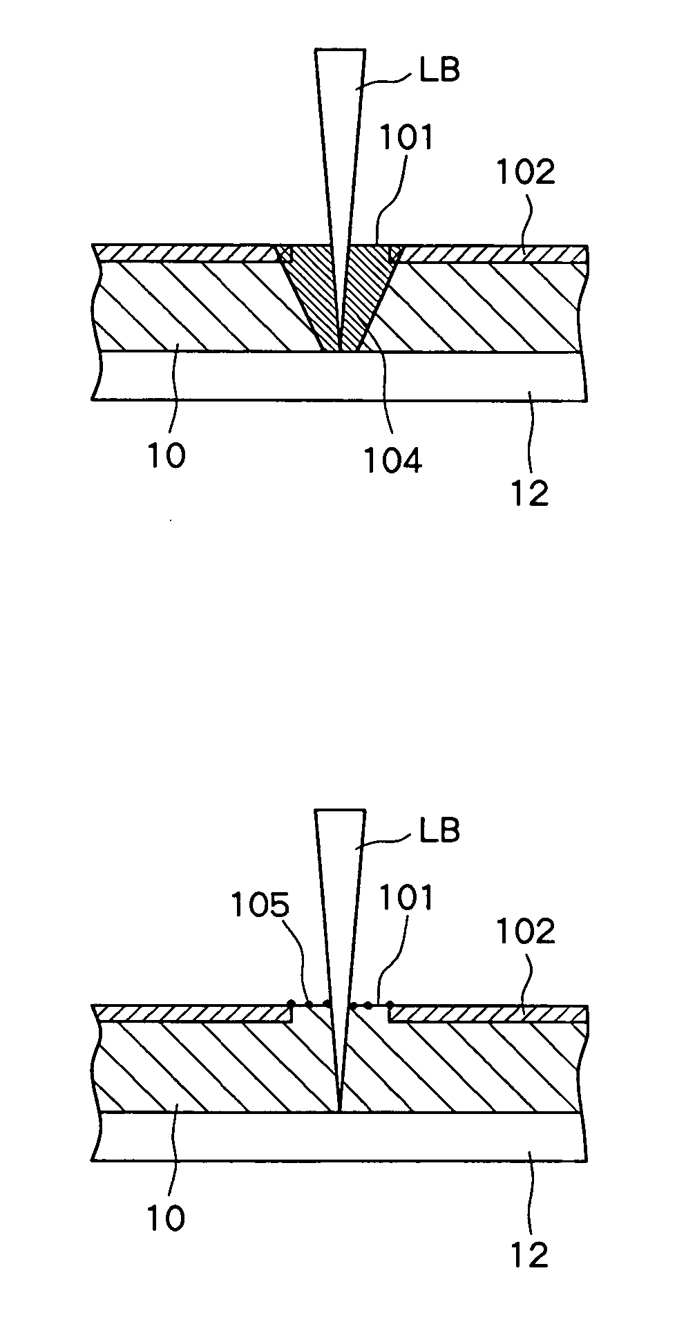
[0022] The method of dividing a semiconductor wafer and the dividing apparatus constituted according to preferred embodiments of the present invention will be described in detail with reference to the accompanying drawings.

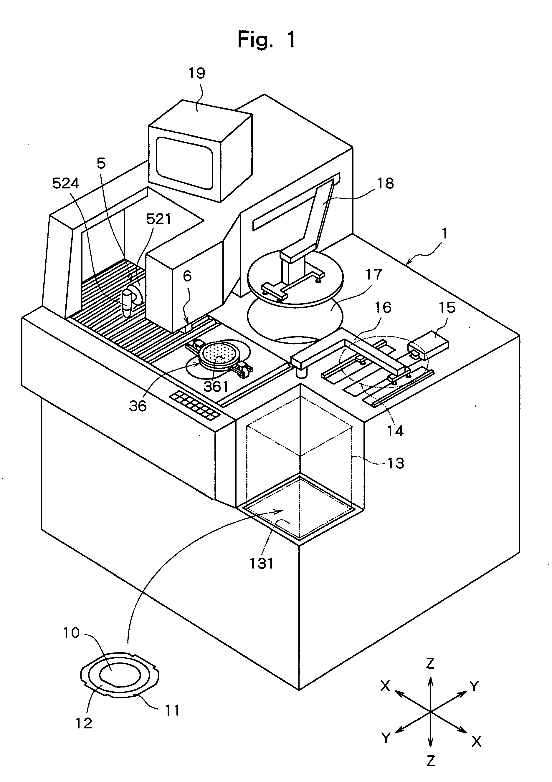
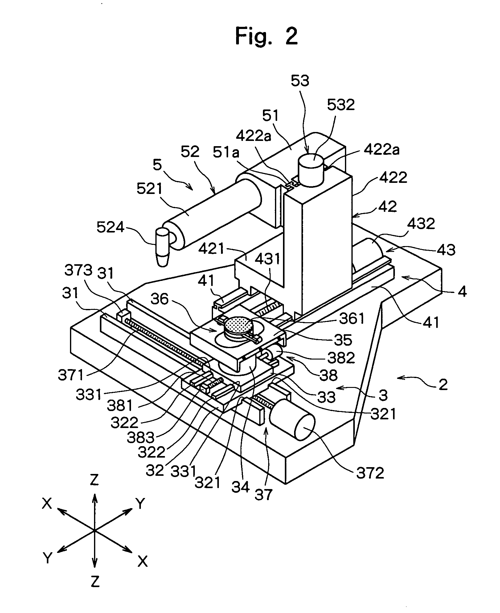
[0023]FIG. 1 is a perspective view of the dividing apparatus for a semiconductor wafer constituted according to the present invention. The dividing apparatus shown in FIG. 1 comprises a substantially rectangular parallelepiped housing 1. Within this housing 1, there are installed a stationary base 2 shown in FIG. 2, a chuck table mechanism 3 for holding a workpiece, which is mounted on the stationary base 2 in such a manner that it can move in a direction shown by an arrow X, a laser beam unit support mechanism 4 mounted on the stationary base 2 in such a manner that it can move in a direction shown by an arrow Y perpendicular to the direction shown by the arrow X, and a laser beam unit 5 mounted on the laser beam unit support mechanism 4 in such a manner that it...


PUM

PropertyMeasurementUnit
diameteraaaaaaaaaa
thicknessaaaaaaaaaa
thicknessaaaaaaaaaa

Abstract

A method of dividing a semiconductor wafer having circuits formed in a plurality of areas defined by streets arranged on the front surface in a lattice form along the streets, comprising the step of detecting the streets from the back surface of the semiconductor wafer and the step of cutting the semiconductor wafer along the streets detected in the street detection step by applying a laser beam to the back surface of the semiconductor wafer along the streets.

Description

TECHNICAL FIELD [0001] The present invention relates to a method of dividing a semiconductor wafer into individual semiconductor chips by exposing the semiconductor wafer to a laser beam along predetermined streets (cutting lines), and to a dividing apparatus. BACKGROUND ART [0002] As is known to people of ordinary skill in the art, in the production of a semiconductor device, a plurality of areas are defined by streets (cutting lines) formed on the front surface of a substantially disk-shaped semiconductor wafer in a lattice form, and a circuit such as IC or LSI is formed in each of the defined areas. The semiconductor wafer is cut along the streets to separate the areas having circuit formed therein from one another, thereby manufacturing individual semiconductor chips. Cutting along the streets of the semiconductor wafer is generally carried out by a cutting machine called “dicer”. This cutting machine has a chuck table for holding a semiconductor wafer as a workpiece, a cutting ...

Claims


Application Information

Patent Timeline
Patent Type & Authority Applications(United States)
IPC IPC(8): B23K26/38B23K101/40H01L21/00H01L21/301H01L21/78B23K26/40
CPCB23K26/04H01L21/78H01L21/67092B23K26/4075B23K26/40B23K2103/50H01L21/30B23K23/00
Inventor NAGAI, YUSUKE
Owner DISCO CORP
Why Eureka
Try Eureka