Threading-dislocation-free nanoheteroepitaxy of Ge on Si using self-directed touch-down of Ge through a thin SiO2 layer

a nano-heteroepitaxy and sio2 layer technology, applied in the direction of crystal growth process, polycrystalline material growth, chemically reactive gas growth, etc., can solve the problems of degrading semiconductor device performance and impracticality of using the heteroepitaxy layer

Active Publication Date: 2005-03-10
STC UNM
View PDF14 Cites 102 Cited by
  • Summary
  • Abstract
  • Description
  • Claims
  • Application Information

AI Technical Summary

Problems solved by technology

A lattice mismatched epitaxial layer at a semiconductor interface can lead to a high density of dislocations that degrade semiconductor device performance.
Problems arise, however, because an epitaxial layer of a lattice-mismatched material on a substrate is often limited to a critical thickness (hc), before misfit dislocations begin to form in the expitaxial material.
Because of the relatively small hc and the large dislocation densities at thicknesses greater than hc, use of the heteroepitaxial layer is impractical.

Method used


Image

  • Threading-dislocation-free nanoheteroepitaxy of Ge on Si using self-directed touch-down of Ge through a thin SiO2 layer
  • Threading-dislocation-free nanoheteroepitaxy of Ge on Si using self-directed touch-down of Ge through a thin SiO2 layer
  • Threading-dislocation-free nanoheteroepitaxy of Ge on Si using self-directed touch-down of Ge through a thin SiO2 layer

Examples


example 1

[0032] Samples I was undoped Si(100) including an interface layer of SiO2. Sample II was undoped Si(100) stripped of an interface layer by exposure to HF.

[0033] Both sample substrates were first treated to remove contaminates by immersion in a Piranha solution for about 5 minutes to form a thin layer of SiO2 on the substrate. The Piranha solution was prepared by mixing 4 volumetric parts of 2M H2SO4 with 1 volumetric part of 30 wt % H2O2. The samples were then treated for 5 minutes in an HF solution to remove the SiO2 layer. The HF solution was prepared by diluting a 49 wt % electronics grade HF solution to 11 wt % by deionized H2O. The Piranha-HF treatments were repeated three times.

[0034] A fresh Piranha solution was prepared and Sample I was treated at 80° for 10 minutes to form a thin layer of chemical oxide. After treatment, Sample I was rinsed with deionized H2O, and blow-dried with N2. No chemical oxide layer was formed on Sample II.

[0035] Sample I was then immediately loa...


PUM

PropertyMeasurementUnit
temperatureaaaaaaaaaa
widthaaaaaaaaaa

Abstract

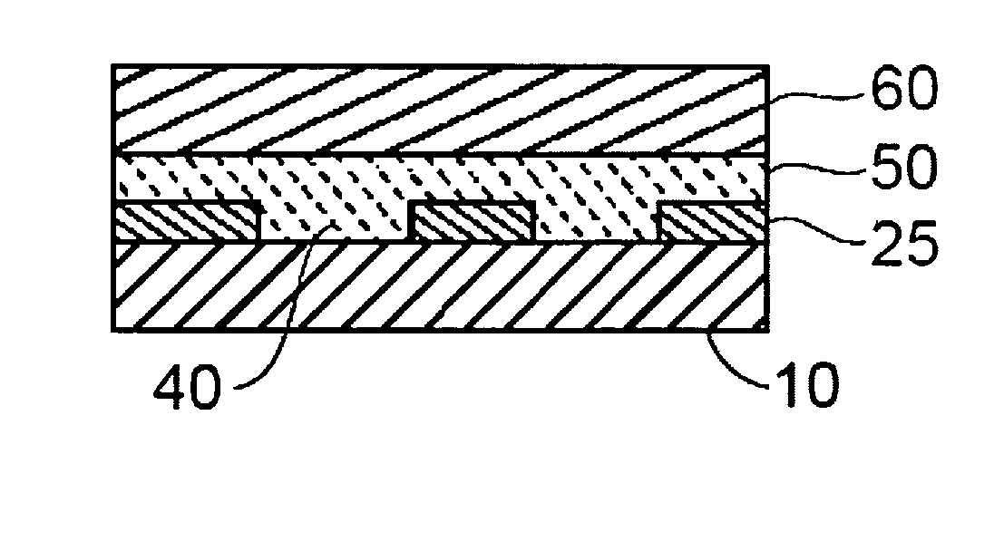
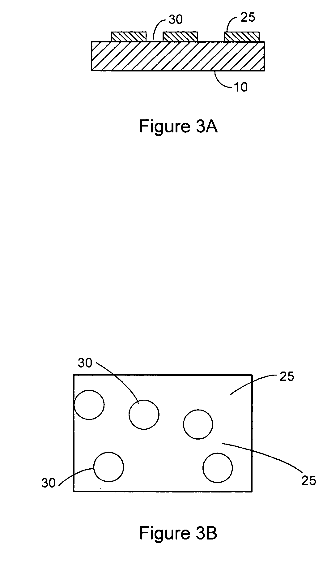
A method of forming a virtually defect free lattice mismatched nanoheteroepitaxial layer is disclosed. The method includes forming an interface layer on a portion of a substrate. A plurality of seed pads are then formed by self-directed touchdown by exposing the interface layer to a material comprising a semiconductor material. The plurality of seed pads, having an average width of about 1 nm to 10 nm, are interspersed within the interface layer and contact the substrate. An epitaxial layer is then formed by lateral growth of the seed pads over the interface layer.

Description

CROSS-REFERENCE TO RELATED APPLICATIONS [0001] This application claims priority to U.S. Provisional Patent Application Ser. No. 60 / 501,274 filed on Sep. 9, 2003, the disclosure of which is incorporated herein by reference.GOVERNMENT RIGHTS [0002] This invention was made with government support under Award No. DMR-0094145 awarded by the National Science Foundation. The government has certain rights in the invention.FIELD OF THE INVENTION [0003] The present invention relates to. semiconductor devices and methods for their manufacture and, more particularly, relates to epitaxial growth of lattice mismatched systems. BACKGROUND OF THE INVENTION [0004] Conventional semiconductor device fabrication is generally based on growth of lattice-matched layers. A lattice mismatched epitaxial layer at a semiconductor interface can lead to a high density of dislocations that degrade semiconductor device performance. Over the past several years, however, there has been increased interest in epitaxia...

Claims


Application Information

Patent Timeline
Patent Type & Authority Applications(United States)
IPC IPC(8): H01L21/20H01L27/01
CPCH01L21/02381H01L21/0245H01L21/02647H01L21/02532H01L21/02642H01L21/02521
Inventor HAN, SANGLI, QIMING
Owner STC UNM
Why Eureka
Try Eureka