Surface light emitting element, optical module, light transmission device
- Summary
- Abstract
- Description
- Claims
- Application Information
AI Technical Summary
Benefits of technology
Problems solved by technology
Method used
Image

Examples
first exemplary embodiment
[0050] 1. Structure of Surface Light Emitting Element
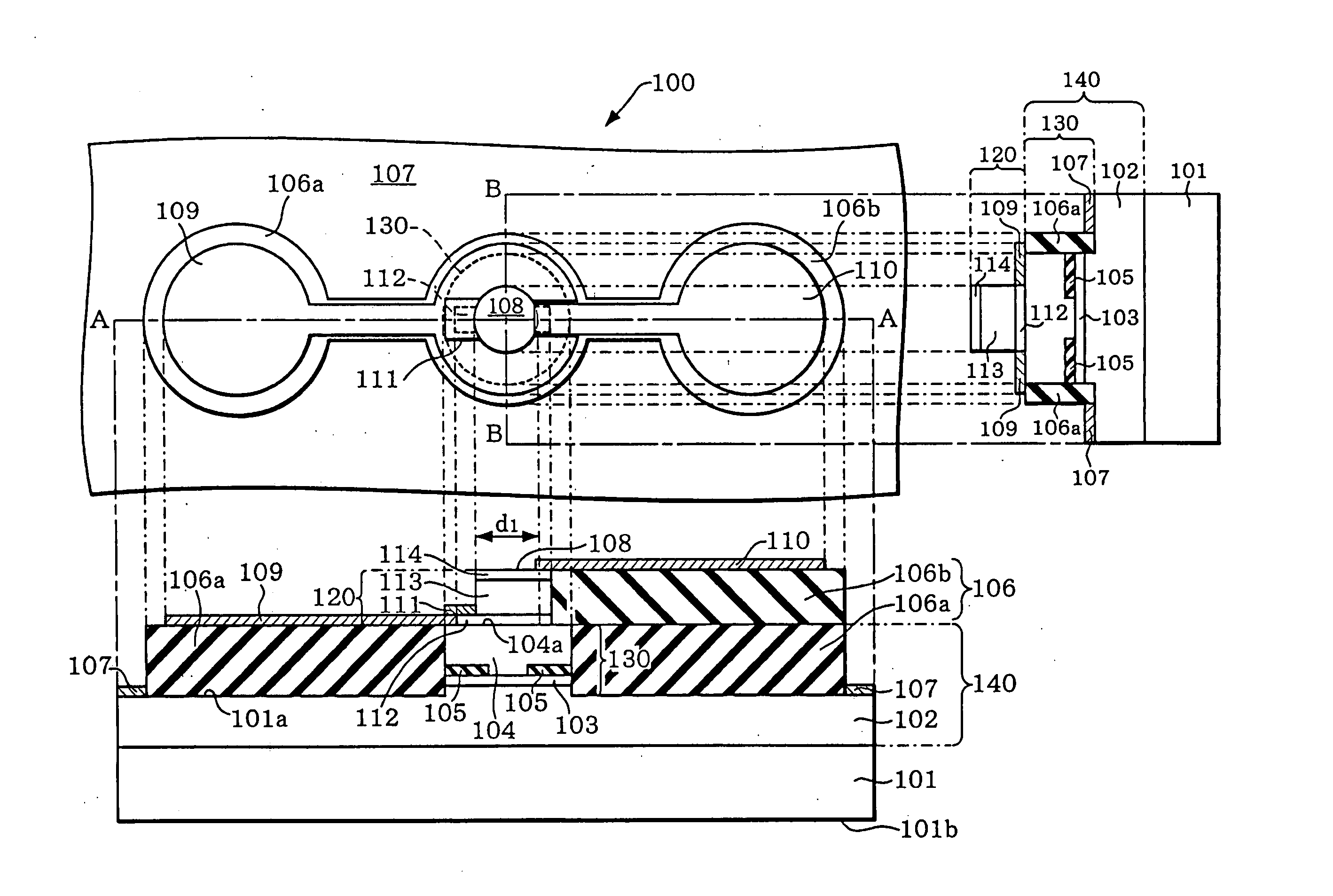
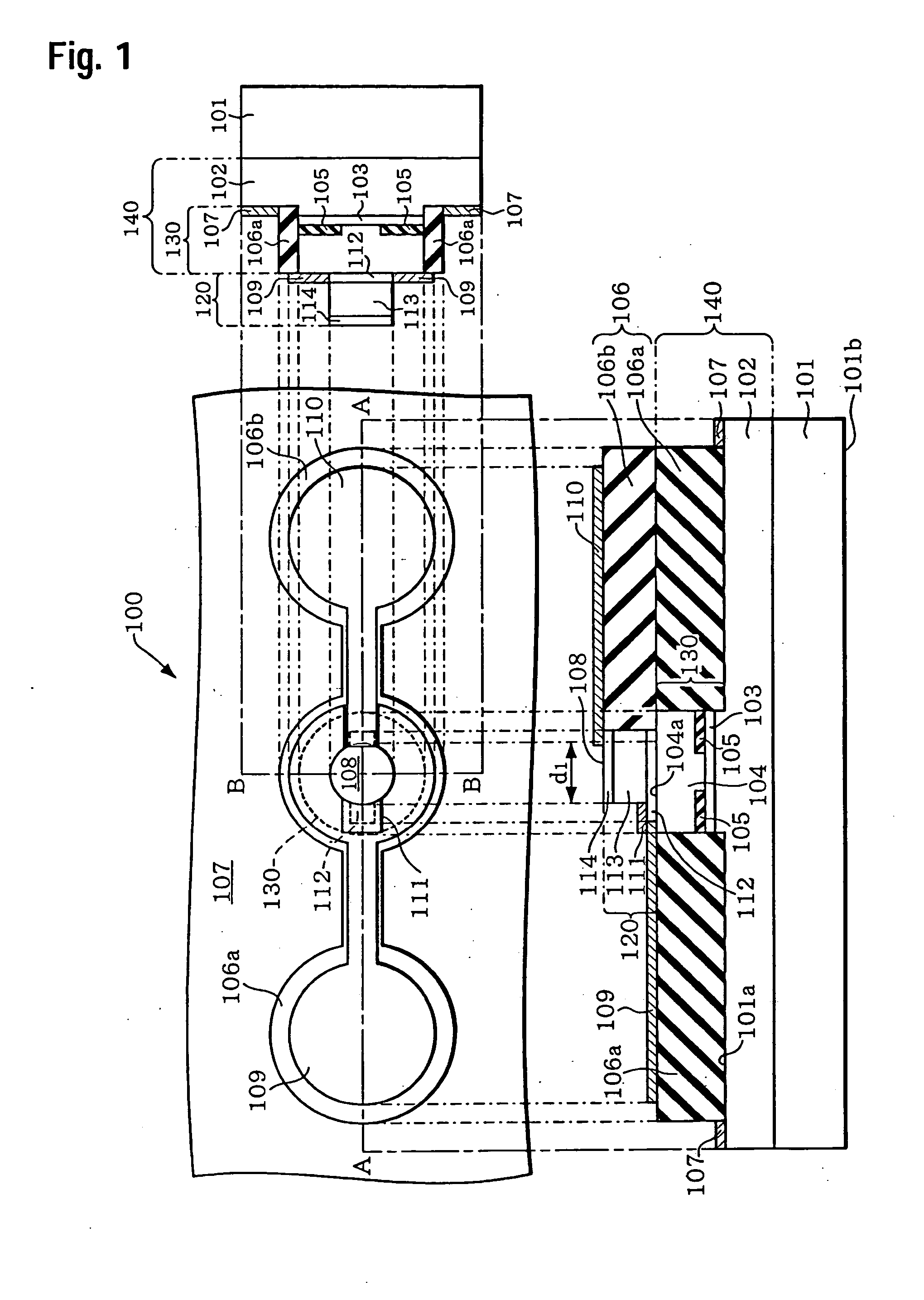
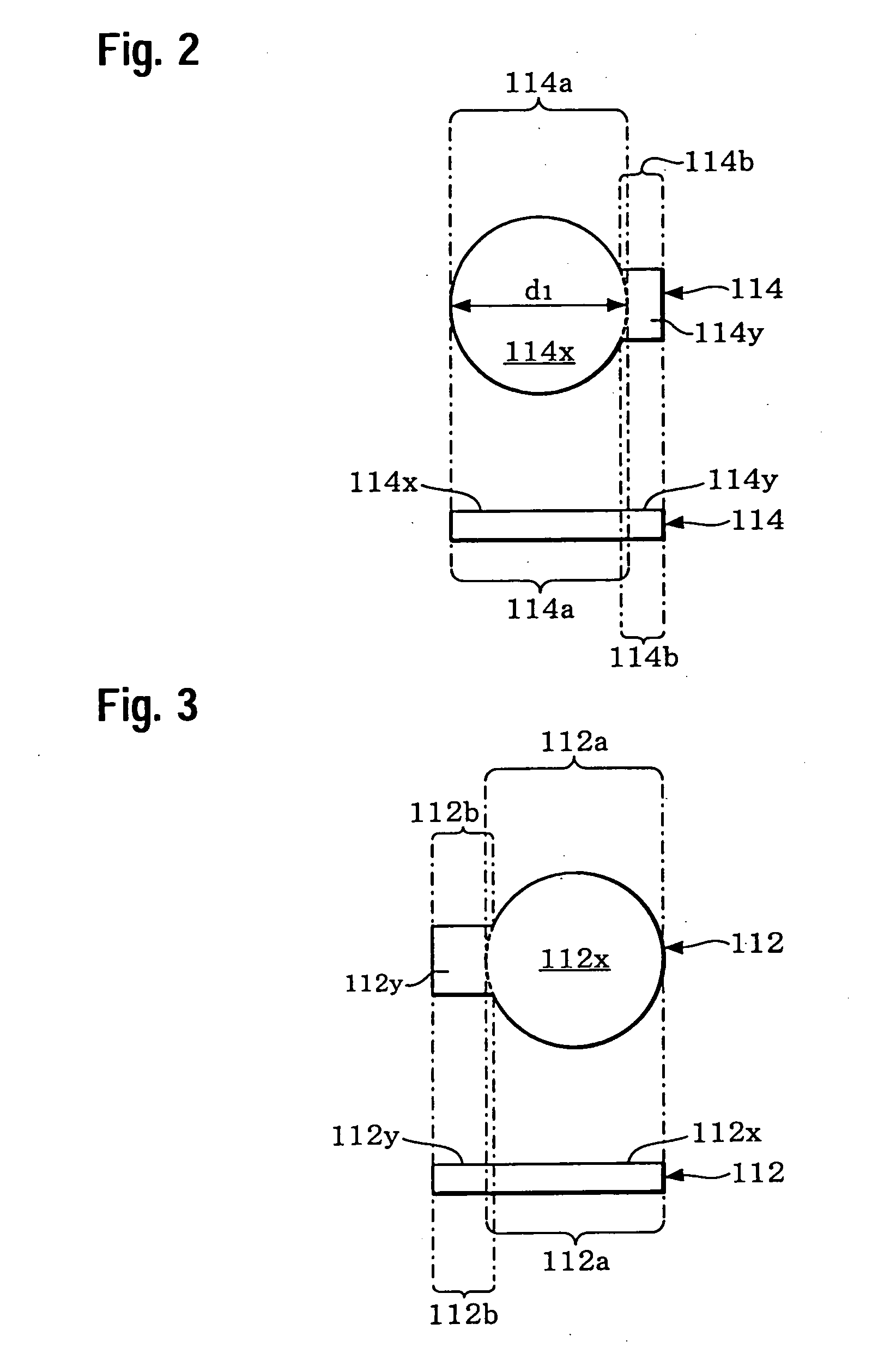
[0051]FIG. 1 shows a schematic and cross-sectional schematic explaining a surface light emitting element 100 according to a first exemplary embodiment applying the present invention. In FIG. 1, a schematic and cross-sectional schematic along the A-A plane and the B-B plane of the 1 are shown. FIG. 2 shows a schematic and a cross-sectional schematic explaining the first contact layer 114 shown in FIG. 1 by enlarging. FIG. 3 shows a schematic and a cross-sectional schematic explaining the second contact layer 112 shown in FIG. 1 by enlarging. FIG. 4 shows a schematic and cross-sectional schematic explaining a first electrode 110, a second electrode 111, a third electrode 109 and a fourth electrode 107 shown in FIG. 1 by enlarging. Furthermore, in FIG. 2 and FIG. 3, only the first contact layer 114 and the second contact layer 112 are excerpted for description.
[0052] As shown in FIG. 1, the surface light emitting element 100 accord...
second exemplary embodiment
[0149] 1. Structure of Surface Light Emitting Element
[0150]FIG. 15 shows a schematic and cross sectional schematics explaining a surface light emitting element 200 according to a second exemplary embodiment applying the present invention. FIG. 16 shows a schematic and a cross sectional schematic explaining a second contact layer 212 shown in FIG. 15 by enlarging. FIG. 17 shows a schematic and a cross sectional schematic explaining a second contact layer 212 and a second electrode 211 shown in FIG. 15 by enlarging. As for the exemplary embodiment, a case that the surface light emitting semiconductor laser is used as the surface light emitting element will be described, which is similar to the first exemplary embodiment.
[0151] The surface light emitting element 200 according to the exemplary embodiment generally has the same structure as the surface light emitting element 100 according to the first exemplary embodiment except that a plurality of the second coupling parts 212b and sec...
third exemplary embodiment
[0160] 1. Structure of Surface Light Emitting Element
[0161]FIG. 19 shows a schematic and cross sectional schematics explaining a surface light emitting element 300 according to a third exemplary embodiment. As for the exemplary embodiment, a case that the surface light emitting semiconductor laser is used as the surface light emitting element will be described, which is similar to the first exemplary embodiment and the second exemplary embodiment.
[0162] The surface light emitting element 300 according to the exemplary embodiment has a different structure from the surface light emitting element 100 according to the first exemplary embodiment in that a light detecting part 320 includes a second contact layer 312, formed of p-type GaAs, and a first contact layer 314, formed of n-type GaAs. The second electrode coupling part is not provided to the second contact layer 312, and the third electrode 109 also functions as a second electrode. Except for the above points, it has generally t...
PUM
 Abstract
Description
Claims
Application Information
 - Generate Ideas
- Intellectual Property
- Life Sciences
- Materials
- Tech Scout
- Unparalleled Data Quality
- Higher Quality Content
- 60% Fewer Hallucinations
Browse by: Latest US Patents, China's latest patents, Technical Efficacy Thesaurus, Application Domain, Technology Topic, Popular Technical Reports.
© 2025 PatSnap. All rights reserved.Legal|Privacy policy|Modern Slavery Act Transparency Statement|Sitemap|About US| Contact US: help@patsnap.com