Check patentability & draft patents in minutes with Patsnap Eureka AI!

Group III nitride based quantum well light emitting device structures with an indium containing capping structure

a quantum well and capping technology, applied in the field of microelectronic devices, can solve the problems of uneven crystal lattice between the crystal lattice of the substrate and the gallium nitride, aluminum nitride is insulating rather than conductive, and the thickness of the epitaxial layer is increased

Inactive Publication Date: 2005-03-17
CREELED INC
View PDF39 Cites 90 Cited by
  • Summary
  • Abstract
  • Description
  • Claims
  • Application Information

AI Technical Summary

Benefits of technology

The present invention provides Group III nitride based light emitting devices and methods of fabricating them that include an n-type Group III nitride layer, a Group III nitride based active region on the n-type Group III nitride layer, and a p-type Group III nitride layer including aluminum on the active region. The devices also include a first contact on the n-type Group III nitride layer and a second contact on the p-type Group III nitride layer. The devices may also include a silicon carbide substrate and a first contact on the substrate opposite the n-type AlGaN layer. The technical effects of the invention include improved device performance and stability, as well as simplified fabrication processes.

Problems solved by technology

One difficulty in fabricating Group III nitride based LEDs, such as gallium nitride based LEDs, has been with the fabrication of high quality gallium nitride.
Such substrates may result in mismatches between the crystal lattice of the substrate and the gallium nitride.
Typically, however, aluminum nitride is insulating rather than conductive.
Typically, eliminating the shorting contact reduces the epitaxial layer thickness, decreases the number of fabrication steps required to produce devices, reduces the overall chip size, and / or increases the device efficiency.
Nevertheless, although these conductive buffer materials offer these advantages, their crystal lattice match with silicon carbide is less satisfactory than is that of aluminum nitride.
The above described difficulties in providing high quality gallium nitride may result in reduced efficiency the device.

Method used


Image

  • Group III nitride based quantum well light emitting device structures with an indium containing capping structure
  • Group III nitride based quantum well light emitting device structures with an indium containing capping structure
  • Group III nitride based quantum well light emitting device structures with an indium containing capping structure

Examples


Embodiment Construction

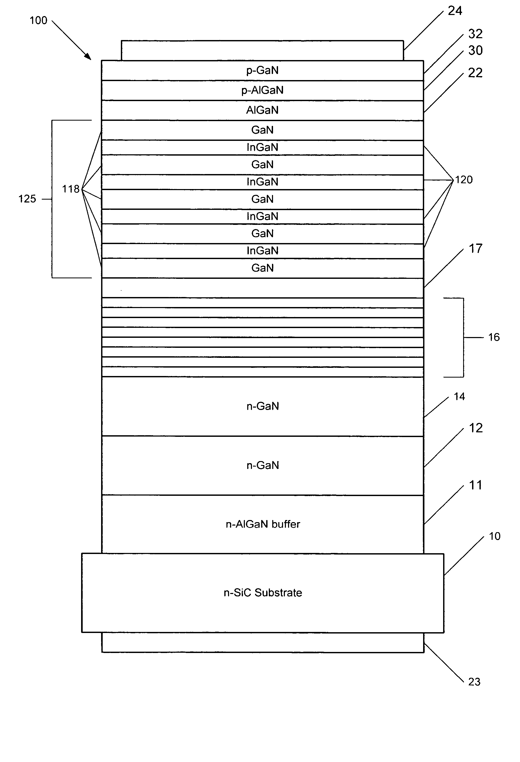
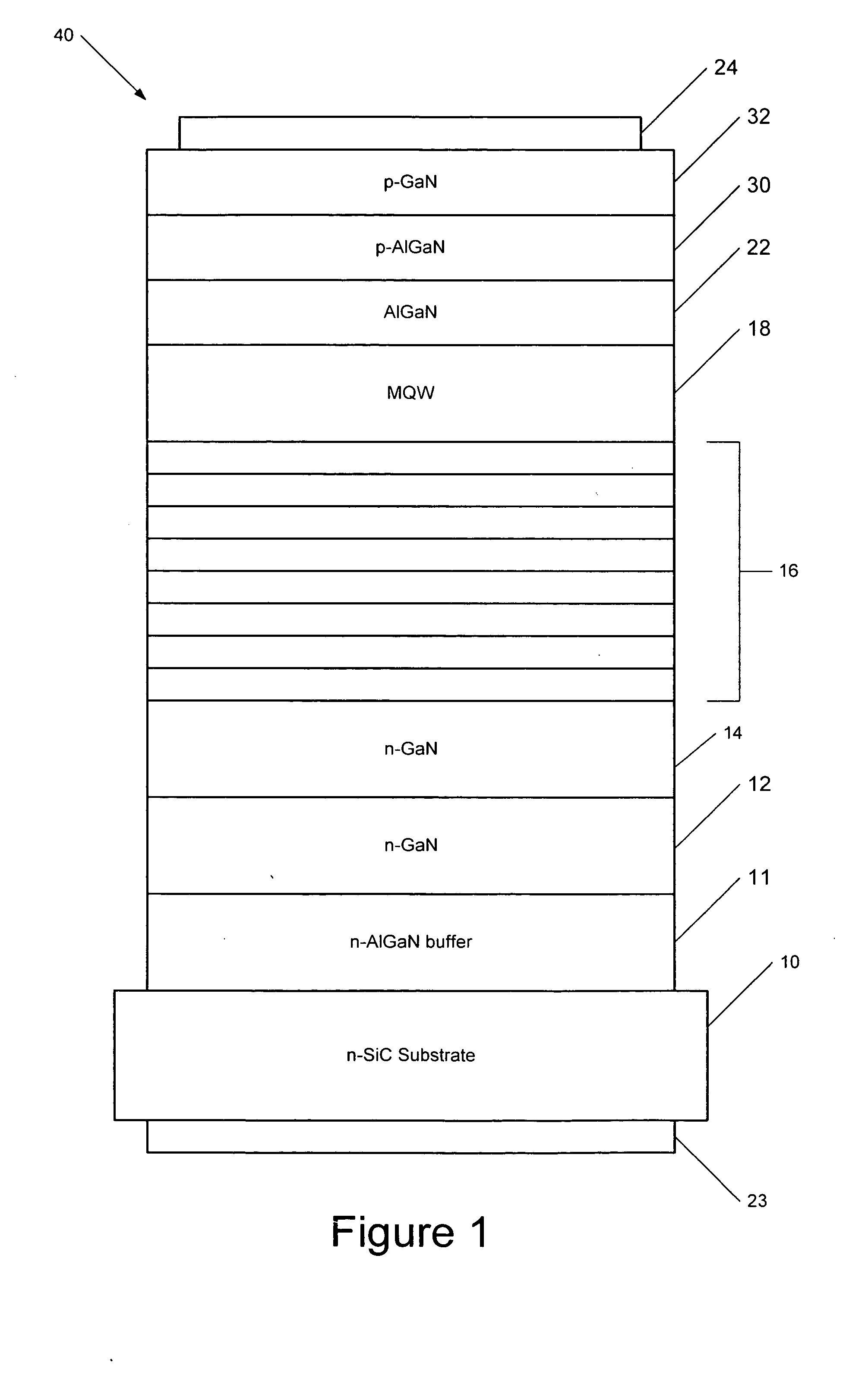
[0022] The present invention now will be described more fully hereinafter with reference to the accompanying drawings, in which embodiments of the invention are shown. However, this invention should not be construed as limited to the embodiments set forth herein. Rather, these embodiments are provided so that this disclosure will be thorough and complete, and will fully convey the scope of the invention to those skilled in the art. In the drawings, the thickness of layers and regions are exaggerated for clarity. Like numbers refer to like elements throughout. As used herein the term “and / or” includes any and all combinations of one or more of the associated listed items.

[0023] The terminology used herein is for the purpose of describing particular embodiments only and is not intended to be limiting of the invention. As used herein, the singular forms “a”, “an” and “the” are intended to include the plural forms as well, unless the context clearly indicates otherwise. It will be furt...


PUM

PropertyMeasurementUnit
thickaaaaaaaaaa
thickaaaaaaaaaa
thickaaaaaaaaaa

Abstract

Group III nitride based light emitting devices and methods of fabricating Group III nitride based light emitting devices are provided. The emitting devices include an n-type Group III nitride layer, a Group III nitride based active region on the n-type Group III nitride layer and comprising at least one quantum well structure, a Group Ill nitride layer including indium on the active region, a p-type Group III nitride layer including aluminum on the Group III nitride layer including indium, a first contact on the n-type Group III nitride layer and a second contact on the p-type Group III nitride layer. The Group III nitride layer including indium may also include aluminum.

Description

CROSS-REFERENCE TO RELATED APPLICATIONS [0001] This application is a continuation-in-part of U.S. patent application Ser. No. 10 / 140,796 filed May 7, 2002 entitled GROUP III NITRIDE BASED LIGHT EMITTING DIODE STRUCTURES WITH A QUANTUM WELL AND SUPERLATTICE, GROUP III NITRIDE BASED QUANTUM WELL STRUCTURES AND GROUP III NITRIDE BASED SUPERLATTICE STRUCTURES which claims the benefit of, and priority from, Provisional Application Ser. No. 60 / 294,445, filed May 30, 2001 entitled MULTI-QUANTUM WELL LIGHT EMITTING DIODE STRUCTURE, Provisional Application Ser. No. 60 / 294,308, filed May 30, 2001 entitled LIGHT EMITTING DIODE STRUCTURE WITH SUPERLATTICE STRUCTURE and Provisional Application Ser. No. 60 / 294,378, filed May 30, 2001 entitled LIGHT EMITTING DIODE STRUCTURE WITH MULTI-QUANTUM WELL AND SUPERLATTICE STRUCTURE, the disclosures of which are hereby incorporated herein by reference in their entirety as if set forth fully herein.FIELD OF THE INVENTION [0002] This invention relates to mic...

Claims


Application Information

Patent Timeline
Patent Type & Authority Applications(United States)
IPC IPC(8): H01L33/06H01L33/32
CPCB82Y20/00H01L33/32H01L33/06H01L33/04
Inventor BERGMANN, MICHAEL JOHNEMERSON, DAVID TODD
Owner CREELED INC
Features
  • R&D
  • Intellectual Property
  • Life Sciences
  • Materials
  • Tech Scout
  • Unparalleled Data Quality
  • Higher Quality Content
  • 60% Fewer Hallucinations
Learn More