Head assembly, disk unit, and bonding method and apparatus

a technology of disk unit and head assembly, which is applied in the direction of record information storage, auxiliary welding devices, maintaining head carrier alignment, etc., can solve the problems of increasing the risk of the inability to remove extremely small foreign particles of the order of 1 m or less, and the inability to produce additional foreign particles. , to achieve the effect of preventing damage to the first surface of the semiconductor chip when the semiconductor chip is handled, and reducing the risk of damag

Inactive Publication Date: 2005-03-17
TOSHIBA STORAGE DEVICE CORP
View PDF15 Cites 8 Cited by
  • Summary
  • Abstract
  • Description
  • Claims
  • Application Information

AI Technical Summary

Benefits of technology

[0017] A further object of the present invention is to provide a method of producing an integrated circuit chip which is mounted on and forms a part of a head assembly, comprising the steps of (a) adhering a film on a surface of a wafer which has conductor bumps formed thereon, so as to surround portions on the surface of the wafer, including the conductor bumps, which later become chips by a waved shape of the film, (b) dicing the wafer having the film into a plurality of chips, and (c) forming a layer on each of the diced chips. According to the method of the present invention, it is possible to produce the chip having the layer formed on the upper and peripheral side surfaces thereof.
[0018] Another object of the present invention is to provide a method of producing an integrated circuit chip which is mounted on and forms a part of a head assembly, the integrated circuit chip having a main chip body and a layer covering the main chip body, the method comprising the steps of (a) supplying a predetermined amount of resin which has a surface tension smaller than a wetting with respect to the main chip body from a nozzle onto an upper surface of the main chip body, the predetermined amount being larger than an amount of the resin required to form the layer, (b) moving the nozzle near the upper surface of the main chip body to a height corresponding to a thickness of the -layer-which is to be formed, and (c) sucking resin by a suction force smaller than the wetting with respect to the main chip body, so as to remove excess resin, to thereby form the layer which covers the main chip body. According to the method of the present invention, it is possible to efficiently produce the chip which is covered by the layer having a desired thickness.
[0019] Still another object of the present invention is to provide a method of producing an integrated circuit chip which is mounted on and forms a part of a head assembly, the integrated circuit chip having a main chip body, conductor bumps and a layer covering the main chip body, the method comprising the steps of (a) forming the layer on the main chip body and the conductor bumps by evaporation, in a state before crushing pointed tip ends of the conductor bumps, (b) pushing the conductor bumps against a surface to simultaneously crush the pointed tip ends of the conductor bumps and make the layer covering the pointed tip ends to recede, to thereby expose surfaces at the crushed portions of the conductor bumps. According to the method of the present invention, it is possible to produce the chip having bumps with exposed tip ends not covered by the layer which covers the chip.
[0020] A further object of the present invention is to provide a method of producing an integrated circuit chip which is mounted on and forms a part of a head assembly, the integrated circuit chip having a main chip body, conductor bumps and a layer covering the main chip body, the method comprising the steps of (a) adhering a mold release agent on tip ends of the conductor bumps, (b) forming the layer on the entire main chip body including the conductor bumps by evaporation, and (c) removing portions of the layer on the tip ends of the conductor bumps having the mold release agent interposed therebetween, to thereby expose surfaces of the tip ends of the conductor bumps. According to the method of the present invention, it is possible to produce the chip having bumps with exposed tip ends not covered by the layer which covers the chip.
[0021] Another object of the present invention is to provide a bonding apparatus for bonding conductor bumps on a semiconductor chip onto corresponding pads on a substrate by ultrasonic vibration, comprising a stage having a receiving surface for receiving a first surface of the-substrate opposite to a second surface of the substrate provided with the pads, and a bonding unit having an end surface for holding a first surface of the semiconductor chip opposite to a second surface of the semiconductor chip provided with the conductor bumps, and a closing member having a closing surface, where the end surface adheres the first surface of the semiconductor chip by suction via a suction hole which opens at the end surface, and the closing member is movable to close the suction hole at the end surface, so that the closing surface and the end surface form a single flat surface. According to the bonding apparatus of the present invention, it is possible to positively prevent a damage to the first surface of the semiconductor chip when the semiconductor chip is handled.
[0022] Still another object of the present invention is to provide a bonding method for bonding conductor bumps on a semiconductor chip onto corresponding pads on a substrate by ultrasonic vibration, comprising the steps of (a) placing the substrate on a stage having a receiving surface for receiving a first surface of the substrate opposite to a second surface of the substrate provided with the pads, (b) holding and-transporting the semiconductor chip to a bonding position above the stage by a bonding unit, the bonding unit having an end surface for holding a first surface of the semiconductor chip opposite to a second surface of the semiconductor chip provided with the conductor bumps by suction via a suction hole which opens at the end surface, and having a movable closing member having a closing surface which forms a single flat surface together with the end surface when the closing member is moved to close the suction hole at the end surface, (c) pressing the semiconductor chip against the substrate by the end surface in a state where the suction hole at the end surface is-closed by the closing member, and (d) bonding the conductor pads to the corresponding pads by ultrasonic vibration. According to the bonding method of the present invention, it is possible to positively prevent a damage to the first surface of the semiconductor chip when the semiconductor chip is handled.

Problems solved by technology

Materials such as silicon and GaAs which are generally used for a base substrate of the head IC chip 30 are fragile and easily crack or chip, because such materials have crystal orientation and have a high elasticity modulus which makes such materials hard.
Even if the head IC 30 is cleaned at a latter process, it is still impossible to remove extremely small foreign particles on the order of 1 μm or less, for example.
In addition, additional foreign particles may be generated during the cleaning process.
Therefore, when the residual foreign particles scatter from the head IC chip 30 due to vibration or air flow caused by the operation of the disk unit, the foreign particles may cause the head crash, thereby deteriorating the reliability of the disk unit.

Method used


Image

  • Head assembly, disk unit, and bonding method and apparatus
  • Head assembly, disk unit, and bonding method and apparatus
  • Head assembly, disk unit, and bonding method and apparatus

Examples


first embodiment

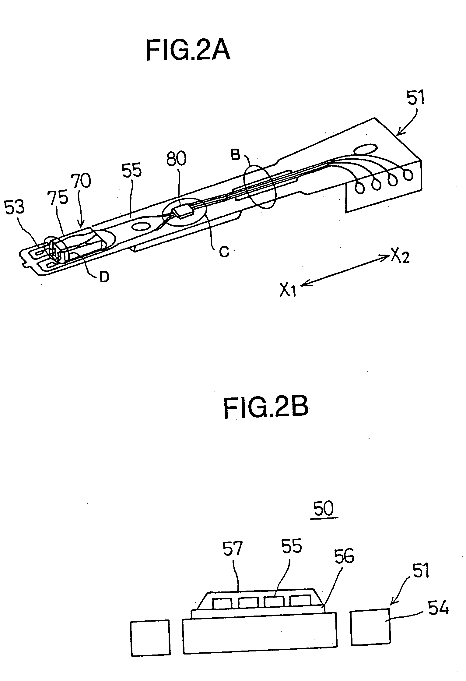
[0089]FIG. 2A is a perspective view showing a first embodiment of a head assembly according to the present invention. FIGS. 2B is a cross sectional view showing an encircled part B of the head assembly shown in FIG. 2A, FIG. 2C is a perspective view showing an encircled part C of the head assembly shown in FIG. 2A, and FIG. 2D is a cross sectional view showing an encircled part D of the head assembly shown in FIG. 2A.

[0090] As shown in FIGS. 2A through 2D, a head assembly 50 includes a head slider 70 which is mounted on a gimbal 52. This gimbal 5.2 is provided on a tip end of a suspension 51 along a direction X1. A head IC chip mounting part 53 is provided at a central part of the suspension 51, and a bear head IC chip 80 is mounted face-down in the head IC chip mounting part 53. In addition, the bear head IC chip 80 is covered by a polymer poly(p-xylylene) evaporated layer 110 which is formed by evaporation. The head IC chip 80 is bear because there is a limit to a projecting heig...

second embodiment

[0112]FIG. 7A is a perspective view showing a second embodiment of the head assembly according to the present invention, and FIG. 7B is a cross sectional view showing an encircled part F of the head assembly shown in FIG. 7A.

[0113] The construction of a head assembly 50A shown in FIG. 7A is basically the same as that of the head assembly 50 shown in FIG. 2A, except for the coverage of the poly(p-xylylene) layer 110. In FIGS. 7A and 7B, those parts which are the same as those corresponding parts in FIGS. 2A and 2D are designated by the same reference numerals, and a description thereof will be omitted.

[0114] As shown on an enlarged scale in FIG. 7B, the poly(p-xylylene) layer 110 of this embodiment covers the upper surface 81b of the main chip body 81, the entirety of the side surfaces 81c, the lower surface 81a, and the peripheries of the Au bumps 84.

[0115] Particularly because the upper surface 81b and the entirety of the side surfaces 81c of the main chip body 81 are covered by...

third embodiment

[0233]FIG. 36A is a perspective view showing a third embodiment of the head assembly according to the present invention. In addition, FIG. 36B is a cross sectional view showing an encircled part G of the head assembly shown in FIG. 36A, and FIG. 36C is a perspective view showing an encircled part H of the head assembly shown in FIG. 36A.

[0234] In a head assembly 50B shown in FIG. 36A, a head IC chip 80C has a structure shown in FIG. 37. FIG. 37 is a perspective view showing the head IC chip 80C shown in FIGS. 36A and 36B. As shown in FIG. 36B, the head IC chip 80C of the head assembly 50B includes a main chip body 81C. As may be seen from FIG. 37, the periphery of a rectangular upper surface 81Cb of the main chip body 81C is chamfered, such that a sloping surface 81Cd is formed between the upper surface 81Cb and each side surface 81Cc of the main chip body 81C.

[0235] Instead of using the poly(p-xylylene) layer 110 shown in FIG. 2D, this embodiment uses a low-viscosity ultraviolet-...


PUM

PropertyMeasurementUnit
thicknessaaaaaaaaaa
heightaaaaaaaaaa
sizeaaaaaaaaaa

Abstract

A head assembly is provided with a mounting surface, and an integrated circuit chip which is mounted on the mounting surface and processes signals. The integrated circuit chip is covered by a layer which prevents generation of foreign particles from the integrated circuit chip by the provision of the layer.

Description

BACKGROUND OF THE INVENTION [0001] 1. Field of the Invention The present invention generally relates to head assemblies, disk units, and bonding methods and apparatuses, and more particularly to a head assembly which is provided with a so-called head IC (Integrated Circuit) chip, a disk unit which uses such a head assembly, and a bonding method and a bonding apparatus which are suited for producing the head assembly and the disk unit. The present invention also relates to semiconductor parts suited for use in head assemblies, and methods of producing such semiconductor parts. [0002] A hard disk unit is made up of a housing which has a sealed structure. The inside of the housing generally includes a hard disk which rotates at a high speed, and a head assembly which is provided on a tip end of an arm which is driven by an actuator. The head assembly has a head slider and a head IC chip which are mounted on a suspension. The head slider includes a magnetic head which is formed by the t...

Claims


Application Information

Patent Timeline
Patent Type & Authority Applications(United States)
IPC IPC(8): G11B5/48H01L21/56H01L21/60H01L21/68H01L23/31H01L29/06
CPCB29C2043/5825G11B5/4806G11B5/486H01L21/56H01L21/563H01L21/568H01L21/6835H01L23/3107H01L24/11H01L24/12H01L24/16H01L24/75H01L24/81H01L24/94H01L29/0657H01L2223/54426H01L2223/5448H01L2224/1134H01L2224/13099H01L2224/13144H01L2224/16225H01L2224/274H01L2224/73203H01L2224/73204H01L2224/73253H01L2224/749H01L2224/75H01L2224/7515H01L2224/75302H01L2224/7565H01L2224/75745H01L2224/75753H01L2224/81801H01L2224/83194H01L2224/83856H01L2924/01005H01L2924/01013H01L2924/01015H01L2924/01029H01L2924/01033H01L2924/0105H01L2924/01074H01L2924/01079H01L2924/01082H01L2924/10158H01L2924/10329H01L2924/14H01L2924/19042H01L2924/30105H01L2924/30107H01L2924/01006H01L2924/01068H01L2924/014H01L24/29H01L2224/32225H01L2924/0132H01L2924/15787H01L24/27H01L2224/29111H01L2224/11822H01L2224/2919H01L2924/00H01L2924/3512H01L2924/00014H01L2224/13111H01L24/05H01L2224/05568H01L2224/05573H01L2224/05624H01L2224/45144H01L2224/73104H01L2924/00011H01L2924/10253H01L2924/12042H01L2924/351G11B5/1272G11B5/40G11B2220/2516
Inventor KIRA, HIDEHIKOBABA, SHUNJIKAINUMA, NORIOOKADA, TORUYAMAKAMI, TAKATOYOSASAKI, YASUNORIKOMIYAMA, TAKESHIKOBAE, KENJIKOBAYASHI, HIROSHI
Owner TOSHIBA STORAGE DEVICE CORP
Why Eureka
Try Eureka