Semiconductor integrated circuit device

a technology of integrated circuits and semiconductors, applied in the direction of information storage, static storage, digital storage, etc., can solve the problems of not being put on the market as wisely, the minimum cell size is limited to 2f4f=8f, and the size of the plate line drive circuit cannot be made larg

Inactive Publication Date: 2005-03-24
KK TOSHIBA
View PDF0 Cites 77 Cited by
  • Summary
  • Abstract
  • Description
  • Claims
  • Application Information

AI Technical Summary

Benefits of technology

[0080]FIG. 48 is a diagram for illustrating a problem of the conventional semiconductor integrated circuit device;
[0081]FIG. 49 is a diagram for illustrating a problem of the conventional semiconductor integrated circuit device;

Problems solved by technology

However, since the flash memory has disadvantages that the number of rewriting operations (the number of W / E operations) is approximately 106, the write time is approximately several micro seconds and application of high voltage (12 V to 22 V) is required for writing, it is not put on the market as wisely as the DRAM.
Therefore, when the wiring width and the distance between the wirings are set to F, there occurs a problem that the minimum cell size is limited to 2F×4F=8F2.
Further, since the pitch of plate line drive circuits is set equal to that of the word lines and is extremely small, the size of the plate line drive circuit cannot be made large.
For this reason, as shown in FIG. 47, the delay time at the time of rise / fall of the plate line potential becomes larger and, as a result, there occurs a problem that the operation speed becomes low.
However, when it becomes higher to some extent, the junction leak at the standby time occurs in a forward direction and the potential stops changing.
However, even in this case, the two leak current amounts have their own distributions.
Therefore, a cell having two bad conditions imposed thereon exists and, as a result, polarization information is destroyed in some cells.
Judging from the above fact, it is difficult to attain the configuration of FIG. 48.
As a result, the conventional ferroelectric memory has a problem that the plate line driving speed is low and the operation speed of the memory is low.
In the memory of the prior application, the following problem occurs.
However, since read charges and write charges move between the cell transistor and the bit line BL via a plurality of cell transistors which are connected in series, delay components of the cell transistors occur.
Therefore, the high-speed operation of the memory is limited.
As described above, in the conventional ferroelectric memory, there occurs a problem that the plate line cannot be commonly used, the high-speed operation cannot be attained and the cell size becomes larger.
Further, in the memory of the prior application, there occurs a problem that the maximum speed is limited by the number of series-connected cells although the cell size can be reduced, the plate line can be commonly used and the high-speed operation can be performed.

Method used


Image

  • Semiconductor integrated circuit device
  • Semiconductor integrated circuit device
  • Semiconductor integrated circuit device

Examples


first embodiment

[0118] (First Embodiment)

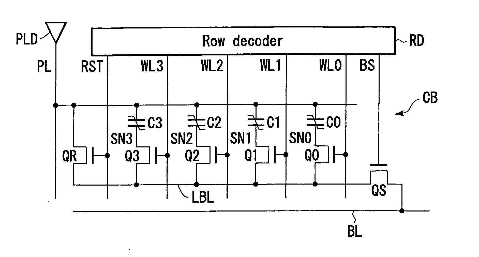
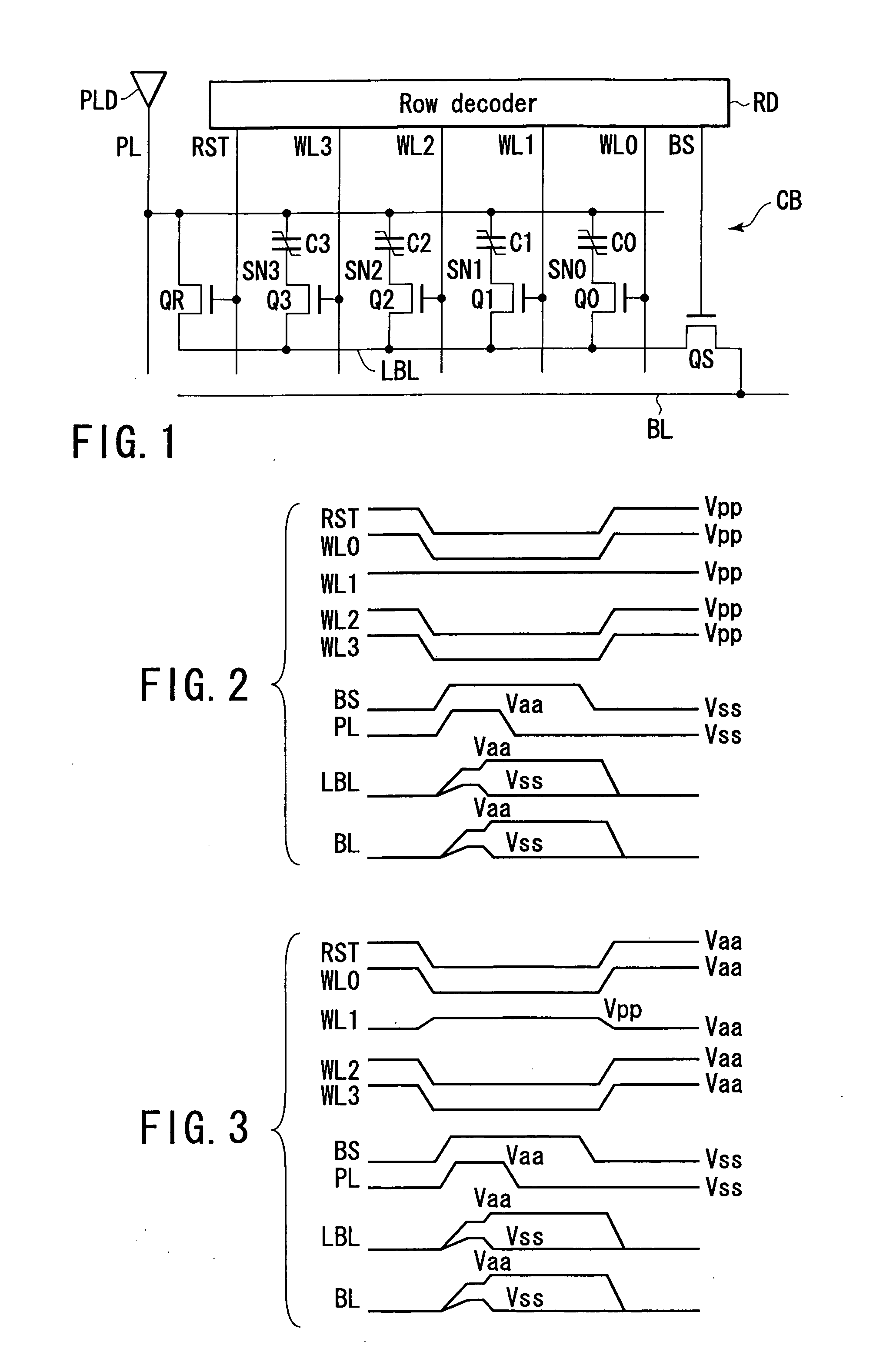
[0119]FIG. 1 shows the circuit configuration of a semiconductor integrated circuit device (FeRAM) according to a first embodiment of the present invention. As shown in FIG. 1, each memory cell includes one cell transistor and one ferroelectric capacitor which are connected in series. That is, the memory cells respectively include cell transistors Q0 to Q3 and ferroelectric capacitors C0 to C3. The gates of the cell transistors Q0 to Q3 are respectively connected to word lines WL0 to WL3. The memory cells are connected in parallel and one end of each memory cell is connected to a plate line PL and the other end thereof is connected to a local bit line LBL.

[0120] A reset transistor QR is connected between the plate line PL and the local bit line LBL. The reset transistor QR is controlled by a reset signal RST. Further, a block selection transistor QS is connected between the local bit line LBL and a bit line BL. The block selection transistor QS is controlled...

second embodiment

[0131] (Second Embodiment)

[0132] A second embodiment relates to one example of the driving method of the plate line PL of the semiconductor integrated circuit device of the first embodiment (FIG. 1). More specifically, the second embodiment relates a case wherein the potential of the plate line PL at the standby time is set to potential Vss and the potential thereof at the drive time is set to internal power supply potential Vaa.

[0133]FIG. 2 shows the operation of the semiconductor integrated circuit device of FIG. 1, for illustrating the second embodiment of the present invention. The operation is explained below by taking a case wherein information is read out from a ferroelectric capacitor C1 as an example.

[0134] As shown in FIG. 2, at the standby time, a reset signal RST and word lines WL0 to WL3 are set at potential Vpp (high level) and a block selection signal BS is set at potential Vss (low level). The plate line PL and bit line BL are set at potential Vss. Therefore, the c...

third embodiment

[0140] (Third Embodiment)

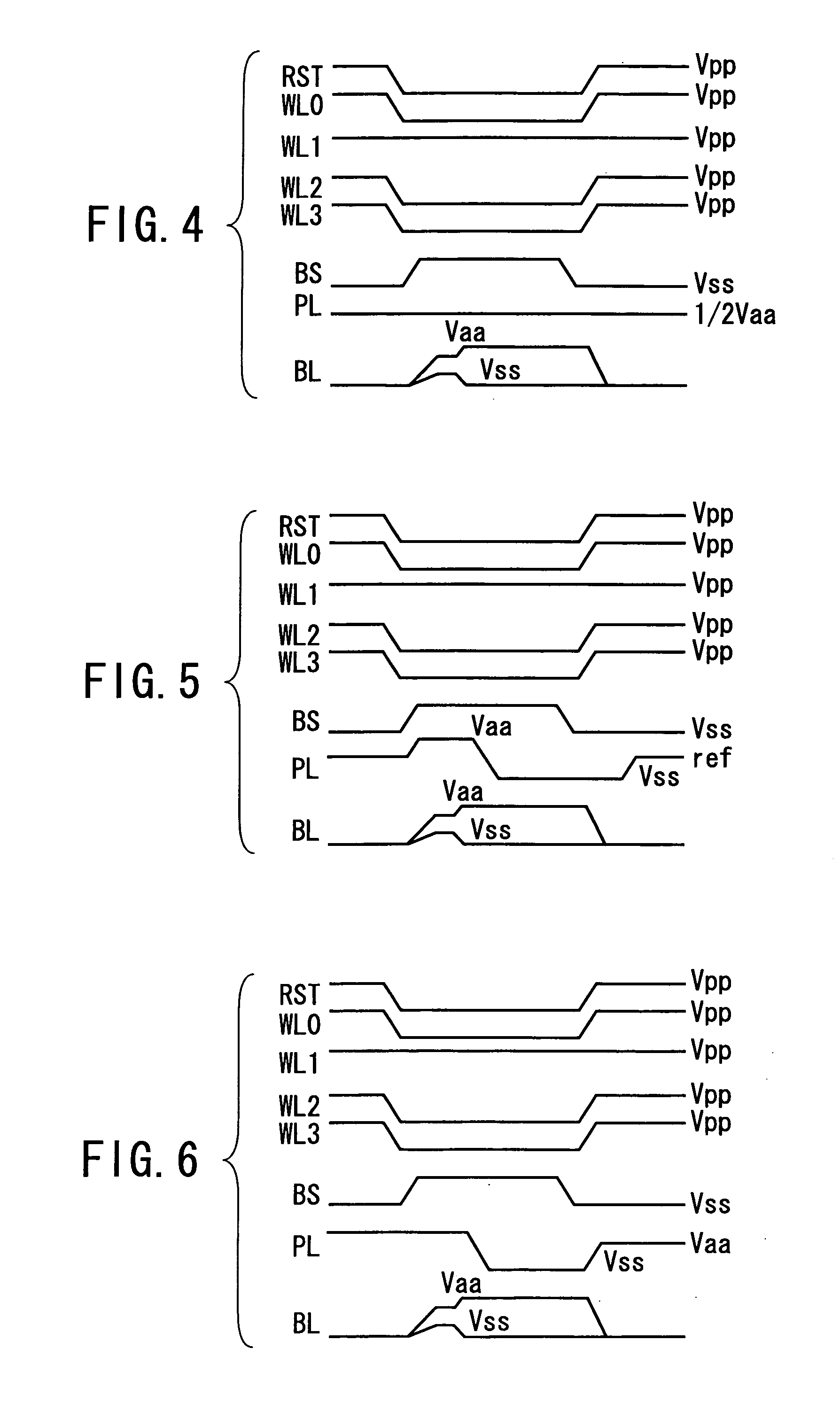
[0141] A third embodiment relates to one example of the driving method of the plate line PL of the semiconductor integrated circuit device of the first embodiment (FIG. 1). More specifically, the third embodiment relates to a case wherein the potential of the plate line PL is fixed at Vaa / 2.

[0142]FIG. 4 shows the operation of the semiconductor integrated circuit device of FIG. 1, for illustrating the third embodiment of the present invention. The operation is explained below by taking a case wherein information is read out from a ferroelectric capacitor C1 as an example.

[0143] As shown in FIG. 4, the state at the standby time is similar to that of the second embodiment except that the plate line PL is driven and set to Vaa / 2. At the active time, a reset signal RST and potentials of the word lines WL0, WL2, WL3 are set to a low level. In this state, the potential (=Vaa / 2) of the plate line PL is applied to one end of the ferroelectric capacitor C1 and the p...


PUM


Abstract

A semiconductor integrated circuit device includes a plurality of first memory cells each of which includes a cell transistor whose gate terminal is connected to a word line and a ferroelectric capacitor which is connected at one end to a source terminal of the cell transistor. The drain terminals of the cell transistors of are used as a first local bit line, the other end of each of the ferroelectric capacitors are used as a first plate line. A first reset transistor has a source terminal connected to the first plate line and a drain terminal connected to the first local bit line. A first block selection transistor has a source terminal connected to the first local bit line and a drain terminal connected to a first bit line.

Description

CROSS-REFERENCE TO RELATED APPLICATIONS [0001] This application is based upon and claims the benefit of priority from prior Japanese Patent Applications No. 2003-329851, filed Sep. 22, 2003; and No. 2003-429163, filed Dec. 25, 2003, the entire contents of both of which are incorporated herein by reference. BACKGROUND OF THE INVENTION [0002] 1. Field of the Invention [0003] This invention relates to a semiconductor integrated circuit device and more particularly to a nonvolatile ferroelectric memory, for example. [0004] 2. Description of the Related Art [0005] At present, semiconductor memories are used in various fields ranging from main memories of large-scale computers to personal computers, home electrical appliances, mobile telephones and the like. Various types of semiconductor memories such as volatile DRAMs (Dynamic Random Access Memories), SRAMs (Static RAMs), nonvolatile MROMs (Mask Read Only Memories) and flash EEPROMs (Electrically Erasable Programmable ROMs) are put on t...

Claims


Application Information

Patent Timeline
Patent Type & Authority Applications(United States)
IPC IPC(8): G11C11/22
CPCG11C11/22
Inventor TAKASHIMA, DAISABURO
Owner KK TOSHIBA
Why Eureka
Try Eureka