Circuit and method for measuring jitter of high speed signals

a high-speed signal and circuit technology, applied in the direction of noise figure or signal-to-noise ratio measurement, instruments, transmission monitoring, etc., can solve the problems of complex and expensive testing, impractical testing, and difficult to accurately measure the timing parameters of circuit signals, so as to achieve accurate measurement of jitter using circuitry, minimal or no impact on the signal under test, and low cost

Active Publication Date: 2005-03-31
SIEMENS PROD LIFECYCLE MANAGEMENT SOFTWARE INC
View PDF13 Cites 94 Cited by
  • Summary
  • Abstract
  • Description
  • Claims
  • Application Information

AI Technical Summary

Benefits of technology

It will be seen that there is a need for a simpler, lower cost technique that accurately measures jitter using circuitry that can tolerate manufacturing process variations and has minimal or no impact on the signal under test.

Problems solved by technology

As the data rate of integrated circuit (IC) signals increases each year, it becomes more difficult to accurately measure timing parameters of the circuit signals.
Jitter is an especially important parameter that is more complex and expensive to test at higher frequencies, to the extent that it is sometimes impractical to test on every circuit manufactured.
Measuring this BER is impossible in a reasonable production test time (less than a few seconds), so measuring the jitter that causes bit errors is often the only alternative.
However, the jitter standard deviation that corresponds to this BER is typically less than ten picoseconds, and is extremely difficult to measure accurately or quickly—a one picosecond error may correspond to 50% error.
Measuring peak-to-peak jitter is unreliable because it is very dependent on the number of samples and measurements are not very repeatable (they may have variance that exceeds 50%) because single-shot events greatly affect the measurement.
Equipment that can measure picosecond jitter is typically quite bulky (more than a cubic foot), and connections between this equipment and a circuit-under-test (CUT) must be made very carefully to minimize the effect on the signal under test and the measurement accuracy.
Connecting measurement equipment to a gigahertz signal typically affects the signal's signal level because of the non-infinite AC impedance of the connection, and affects the signal's jitter because each change in characteristic impedance along the signal's path to the equipment can cause reflections and changes in the signal's transition times.
These are difficult to implement with low jitter (lower jitter than typical gigahertz signals) in the presence of typical circuit manufacturing-process variations and circuit noise.
This technique is too simple for many applications—it only measures peak-to-peak jitter, which is usually too variable to be a reliable parameter for production testing, and requires too long a test time to obtain reliable results for low jitter systems.
This test requires very precise edge placement and high frequencies which add significantly to the complexity and cost of a tester.
In summary, prior art jitter measurement techniques require a precision delay line or analog circuitry, or only measure peak-to-peak jitter, and test equipment is only able to measure the jitter on signals that it can access, and the access connection may increase the jitter.

Method used


Image

  • Circuit and method for measuring jitter of high speed signals
  • Circuit and method for measuring jitter of high speed signals
  • Circuit and method for measuring jitter of high speed signals

Examples


Embodiment Construction

In the following detailed description, numerous specific details are set forth in order to provide a thorough understanding of the present invention. However, it will be understood by those skilled in the art that the present invention may be practiced without these specific details. In other instances, well known methods, procedures, components and circuits have not been described in detail so as not to obscure aspects of the present invention.

An objective of the invention is to test jitter of signal waveforms, relative to predetermined test limits, to determine whether circuitry is free of manufacturing defects. A further objective is to measure the performance of circuitry for purposes of characterization or design validation.

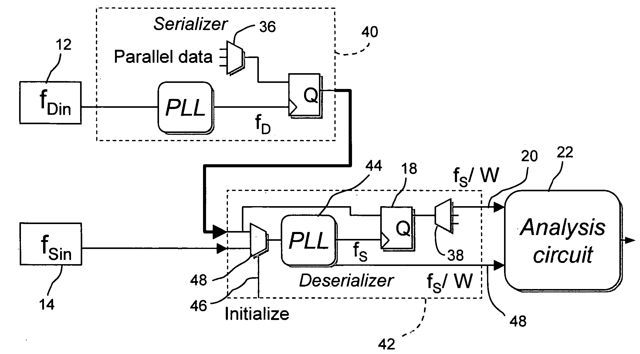
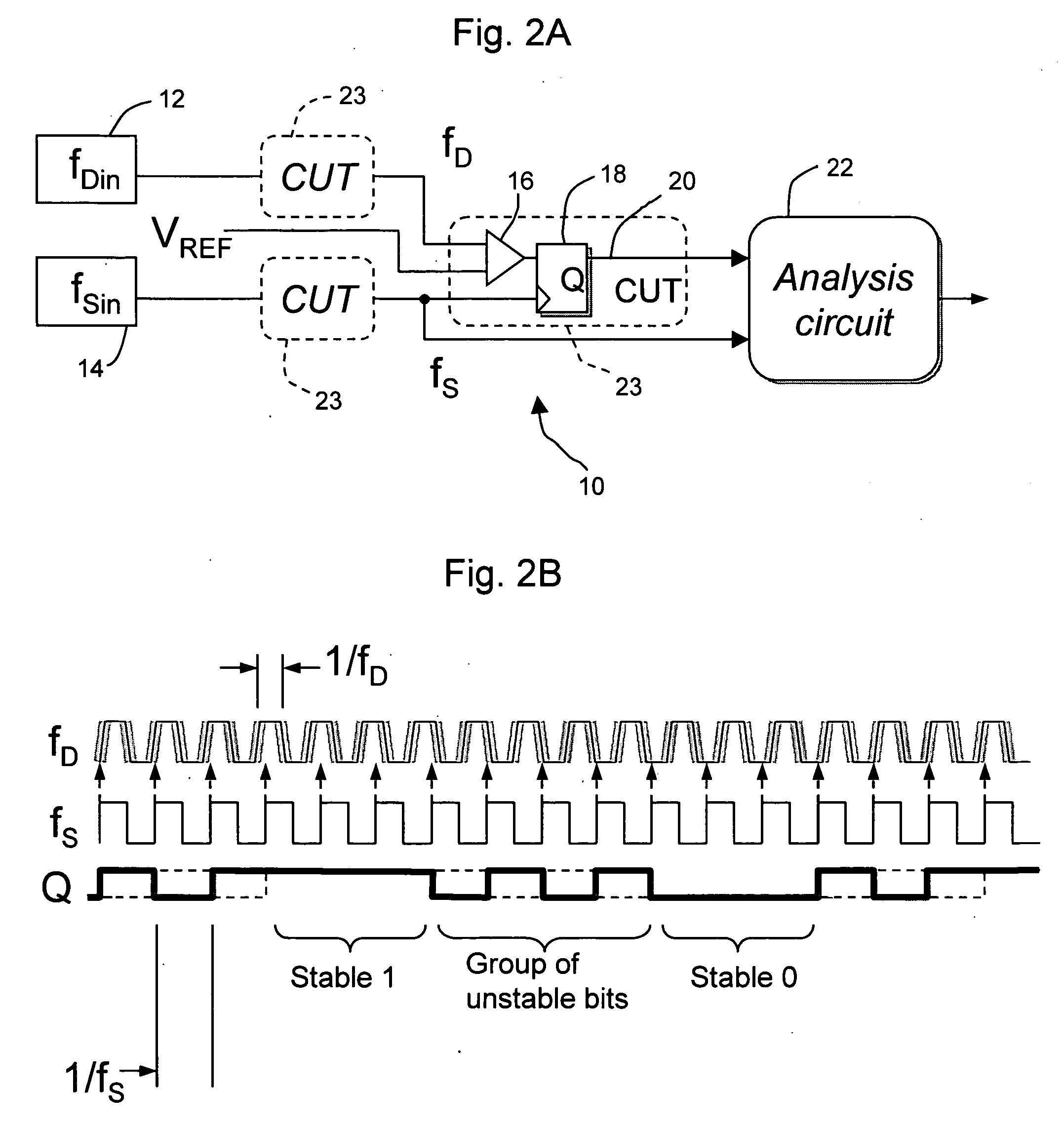
An embodiment of circuit 10 of the present invention is shown in FIG. 2A. The circuit comprises a data clock generator 12 which generates a data signal having a frequency or data rate, fDin, a sampling clock generator 14 which generates a data signal ha...


PUM


Abstract

A method and circuit for measuring a statistical value of jitter for a data signal having a data rate fD, comprises digitally sampling the data signal at a sampling rate, fS, to produce sampled logic values, where fD/fS is a predetermined non-integer ratio; and analyzing the sampled values to deduce a statistical value of the jitter.

Description

BACKGROUND OF THE INVENTION 1. Field of the Invention The present invention relates to test and measurement of signal timing jitter, especially for high-speed digital signals and circuits. 2. Description of Related Art As the data rate of integrated circuit (IC) signals increases each year, it becomes more difficult to accurately measure timing parameters of the circuit signals. Jitter is an especially important parameter that is more complex and expensive to test at higher frequencies, to the extent that it is sometimes impractical to test on every circuit manufactured. For very high speed data transmission (greater than one gigabit per second), the bit error ratio (BER) is typically specified as less than 10−12. Measuring this BER is impossible in a reasonable production test time (less than a few seconds), so measuring the jitter that causes bit errors is often the only alternative. However, the jitter standard deviation that corresponds to this BER is typically less than te...

Claims


Application Information

Patent Timeline
Patent Type & Authority Applications(United States)
IPC IPC(8): H04L1/20H04Q1/20
CPCH04L1/205
Inventor SUNTER, STEPHEN K.ROY, AUBIN P.J.
Owner SIEMENS PROD LIFECYCLE MANAGEMENT SOFTWARE INC
Why Eureka
Try Eureka