

Ferroelectric polymer memory with a thick interface layer
a technology of ferroelectric polymer and interface layer, applied in the field of electromechanical assembly, can solve the problems of insufficient thickness of the interface layer and failure of the device, and achieve the effect of protecting the polymer
- Summary
- Abstract
- Description
- Claims
- Application Information
AI Technical Summary
Problems solved by technology
Method used
Image

Examples
Embodiment Construction
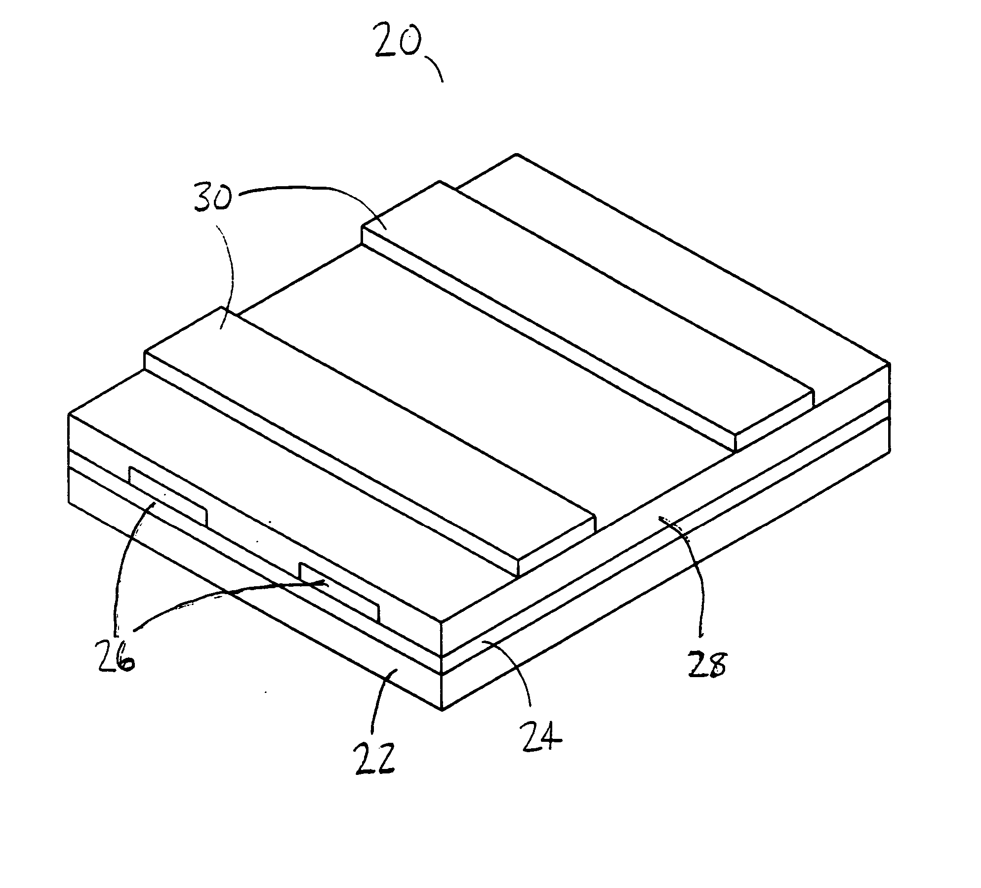
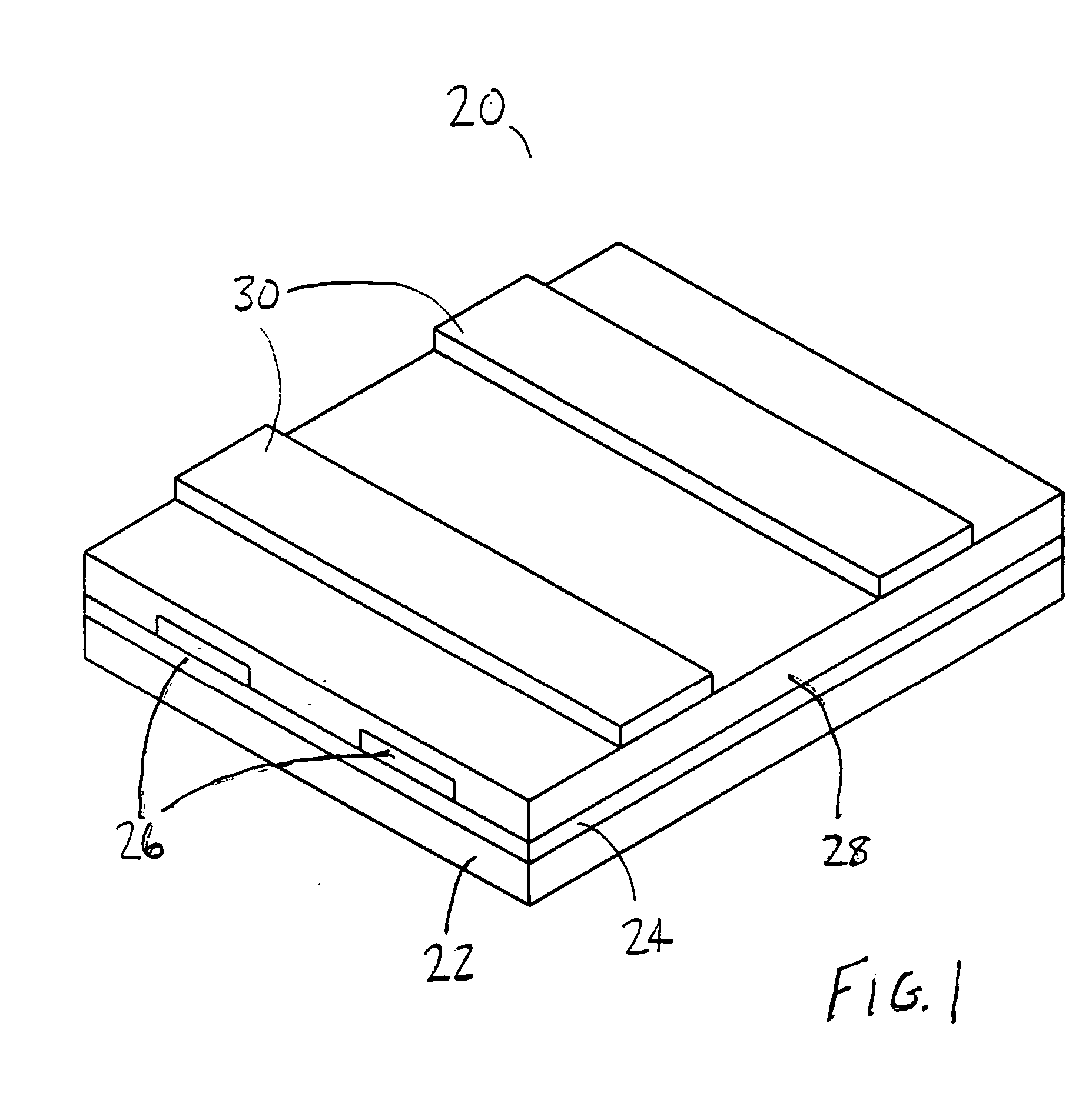
[0021]FIG. 1 to FIG. 8 illustrate a memory array and a method of constructing a memory array. An insulating layer is formed on a semiconductor substrate. A first metal stack is then formed on the insulating layer. The first metal stack is etched to form first metal lines. A polymeric layer is formed over the first metal lines and the insulating layer. The polymeric layer has a surface with a plurality of roughness formations. A second metal stack is formed on the polymeric layer with an interface layer, which is thicker than the heights of the roughness formations. Then the second metal stack is etched to form second metal lines. Memory cells are formed wherever a second metal line extends over a first metal line. Because of the thickness of the interface layer, the polymeric layer is completely separated from rest of the second metal stack.
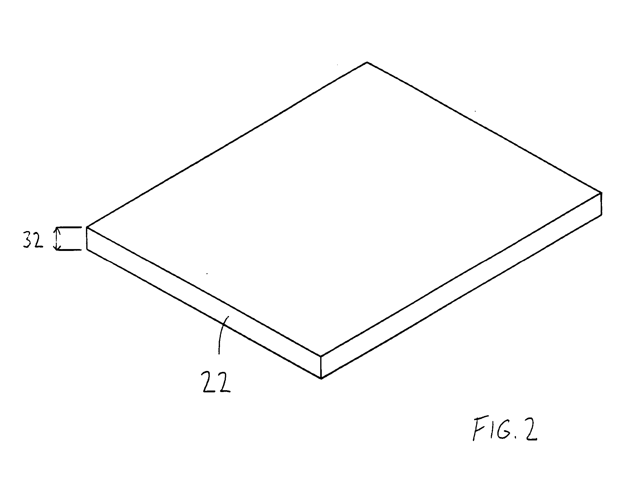
[0022]FIG. 1 illustrates a ferroelectric polymer memory array 20. The memory array 20 may include a substrate 22, an insulating layer 24, lower...
PUM
 Abstract
Description
Claims
Application Information