Semiconductor device having heat conducting plates

a technology of heat conducting plate and semiconductor device, which is applied in the direction of solid-state devices, basic electric elements, other domestic articles, etc., can solve the problems of relatively high production cost of mold b>8/b>, and relatively high production cost of semiconductor device b>1/b>, so as to prevent chip breakage, easy to apply coating resin, and simple structure

Inactive Publication Date: 2005-04-07
DENSO CORP
View PDF26 Cites 16 Cited by
  • Summary
  • Abstract
  • Description
  • Claims
  • Application Information

AI Technical Summary

Benefits of technology

[0007] The present invention has been made in view of the above problems with an object to provide a semiconductor device that makes it possible to use a mold having a simple structure without damaging a semiconductor chip during molding, makes it unnecessary to insulate both outer surfaces of the heat sinks using dedicated insulating sheets after the device is completed, and makes it easier to apply coating resin on a pair of heat sinks in the manufacturing process of the device.
[0008] Insulating sheets, which are made of compressively deformable material, are adhered to the outer surfaces of the heat sinks, and the device is molded in a mold while the sheets are located between the mold and the heat sinks. The sheets are compressively deformed during the molding to prevent the chip from being broken, even if an economical mold having a simple structure is used. The plates are insulated by the sheets to make dedicated insulating sheets unnecessary when the completed device is inspected, screened, or assembled into a unit such as an inverter unit. The coating resin is coated by immersing the chip and the heat sinks in a solution containing the resin to simplify the coating.

Problems solved by technology

A semiconductor chip such as a power IC, which controls a large amount of electric power and current, generates so much heat that a semiconductor device using the chip requires a heat sink to dissipate heat.
Therefore, the structure of the mold 8 is relatively complicated and the production cost of the mold 8 is relatively high.
Thus, the production cost of the semiconductor device 1 is relatively high.
However, in the semiconductor device 1, the distance between the heat sinks 2, 3 is in the range between 1 and 2 mm, so it is difficult to apply the coating resin on the inner surfaces of the heat sinks 2, 3.
It is also difficult to inspect the coating quality.

Method used


Image

  • Semiconductor device having heat conducting plates
  • Semiconductor device having heat conducting plates
  • Semiconductor device having heat conducting plates

Examples


Embodiment Construction

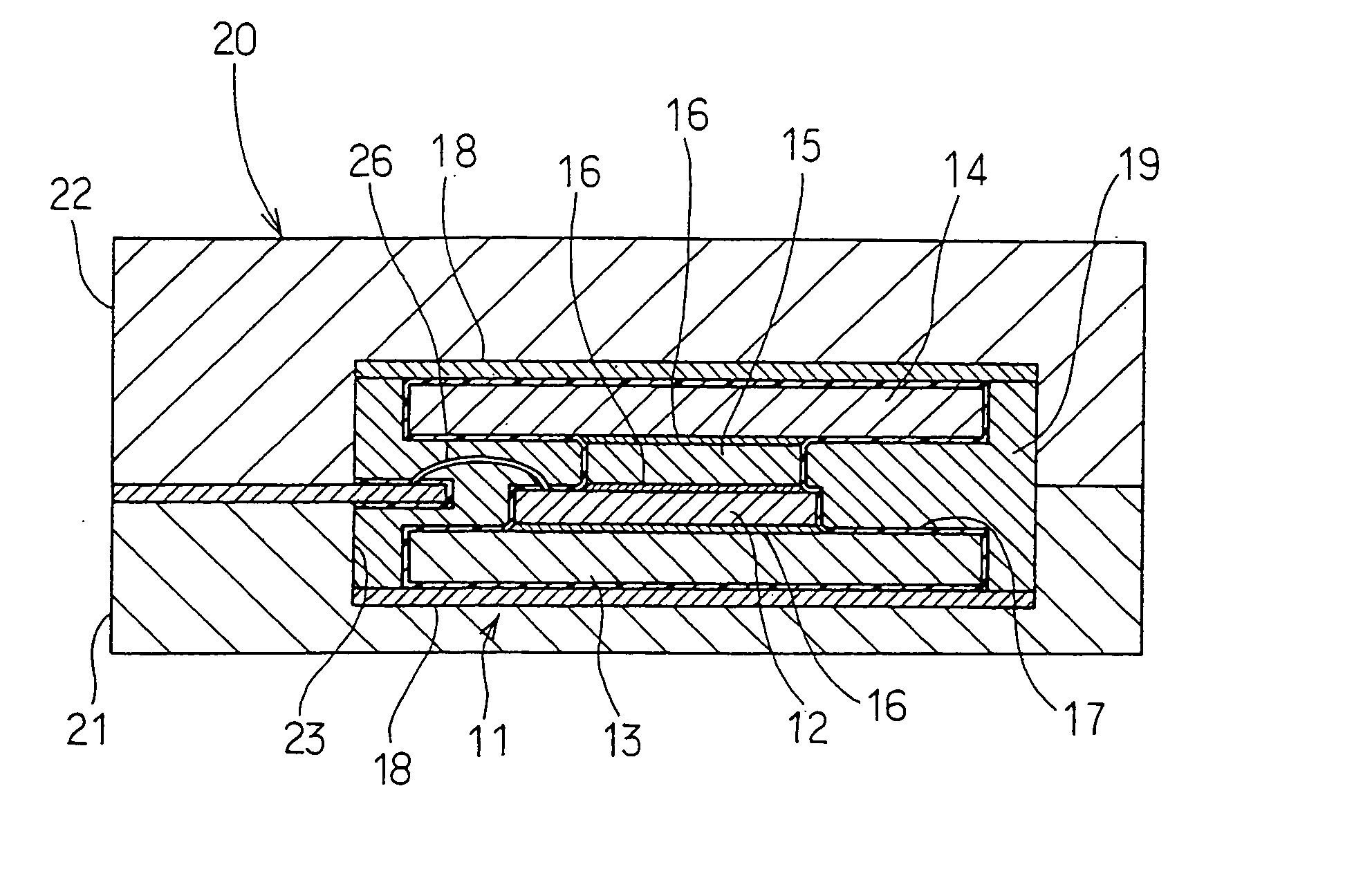
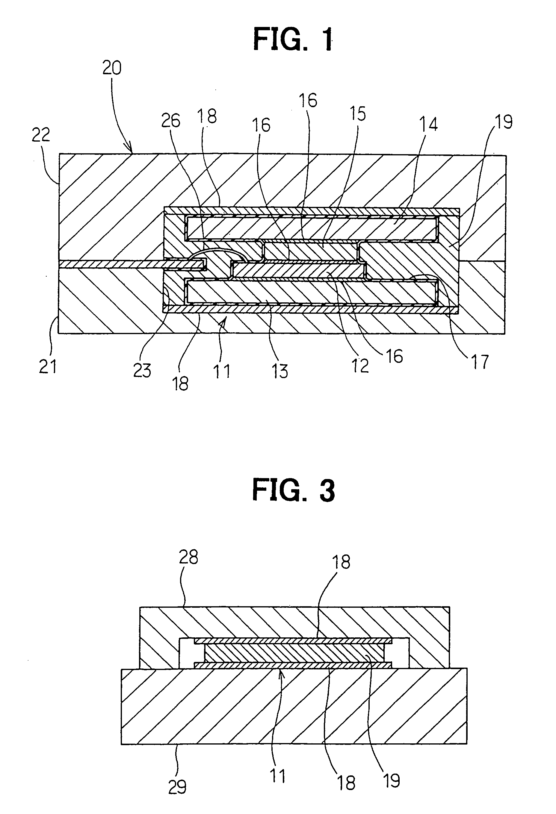
[0019] As shown in FIG. 1, a semiconductor device 11 includes a semiconductor chip 12, which generates heat, a lower heat sink 13 and an upper heat sink 14, which conduct the heat generated by the semiconductor chip, and a heat sink coupler 15. The lower surface of the chip 12 and the upper surface of the lower heat sink 13 are connected by solder 16, the upper surface of the chip 12 and the lower surface of the heat sink coupler 15 are soldered together, and the upper surface of the heat sink coupler 15 and the lower surface of the upper heat sink 14 are soldered together. The heat generated by the chip 12 is conducted through the heat sinks 13 and 14.

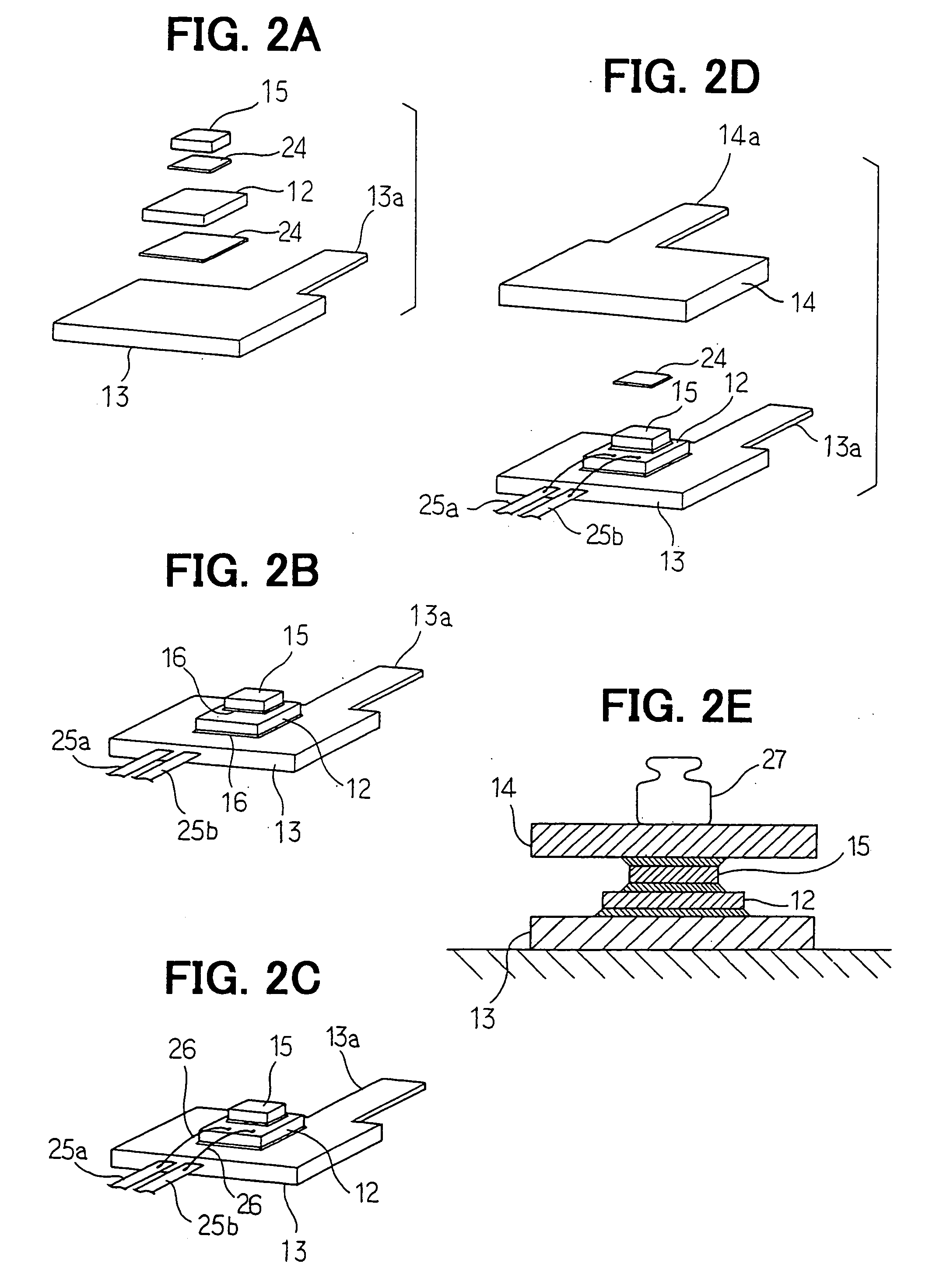
[0020] In this embodiment, the semiconductor chip 12 is a power semiconductor such as an IGBT (Insulated Gate Bipolar Transistor) and a thyristor in the shape of a thin rectangular plate, as shown in FIG. 2A. The lower heat sink 13, the upper heat sink 14, and the heat sink coupler 15 are made of metal having high heat conductivity a...


PUM

PropertyMeasurementUnit
distanceaaaaaaaaaa
distanceaaaaaaaaaa
thicknessaaaaaaaaaa

Abstract

A semiconductor device includes a semiconductor chip generating heat, a pair of heat sinks, which face each other, to conduct heat from both surfaces of the chip, a pair of compressible insulating sheets, and a mold resin covering the chip, the heat sinks, and the sheets such that the sheets are exposed from the surface of the resin. The mold resin is prevented from covering the outer surfaces of the heat sinks, which are pressed by mold parts, and breakage of the chip is avoided during molding. The plates are insulated by the sheets, so no dedicated insulating sheets for the heat sinks are needed after the device is completed.

Description

CROSS REFERENCE TO RELATED APPLICATION [0001] This application is based on and incorporates herein by reference Japanese Patent Application No. 2001-127516, which was filed on Apr. 25, 2001. BACKGROUND OF THE INVENTION [0002] The present invention relates to a semiconductor device in which a semiconductor chip generating heat is located between a pair of heat sinks and to a method for manufacturing the device. [0003] A semiconductor chip such as a power IC, which controls a large amount of electric power and current, generates so much heat that a semiconductor device using the chip requires a heat sink to dissipate heat. As shown in FIG. 4, in a proposed semiconductor device 1, a semiconductor chip 4 and a heat sink coupler 5 are located between a pair of heat sinks 2, 3. One heat sink 2 and the chip 4 are soldered together, the chip 4 and the coupler 5 are soldered together, and the coupler 5 and the other heat sink 3 are soldered together. A mold resin 7 covers the chip 4, the hea...

Claims


Application Information

Patent Timeline
Patent Type & Authority Applications(United States)
IPC IPC(8): B29L31/34H01L21/56B29C45/14H01L23/28H01L23/29H01L23/31H01L23/433
CPCH01L21/565H01L23/3135H01L2924/1305H01L2924/1301H01L2924/01006H01L24/48H01L2924/14H01L2924/13055H01L2924/01082H01L2924/01079H01L2924/01033H01L2924/01029H01L2924/01014H01L2924/01013H01L23/4334H01L24/32H01L24/33H01L24/45H01L2224/32245H01L2224/45124H01L2224/45144H01L2224/48091H01L2224/48247H01L2224/73215H01L2224/73265H01L2924/01004H01L2924/01005H01L2924/00014H01L2924/00H01L2924/181H01L2224/8592H01L2224/83951H01L2224/2612H01L2924/00012
Inventor TESHIMA, TAKANORI
Owner DENSO CORP
Why Eureka
Try Eureka