Optical film, method for manufacturing the same, and phase difference film and polarizing plate using the same

Active Publication Date: 2005-04-07
NITTO DENKO CORP
14 Cites 27 Cited by

AI-Extracted Technical Summary

Problems solved by technology

However, even in a retardation plate having the above-described cholesteric layer, there still is the coloration caused by the selective reflec...

Benefits of technology

Accordingly, the inventors conducted further studies and found the following. A cholesteric layer formed by providing a “liquid crystal monomer,” which will be described later, controlling a blend ratio of this liquid crystal monomer and a chiral dopant, orienting the liquid crystal monomer into a cholesteric structure by the chiral dopant, and then fixing that orientation by polymerization or cross-linking can control the selective reflection wavelength range to be 100 nm to 320 nm. Within this range, it is possible to avoid the conventional problem of light leakage. It should be noted that the inventors found for the first time that using the liquid crystal monomer and controlling the blend ratio made it possible to control the selective reflection wavelength range.
Such an optical film in which the selective reflection wavel...

Abstract

A method for preparing an optical film, which comprises applying and developing an application liquid mixture containing a liquid crystal monomer, a chiral agent and a polymerization initiator on an orientation substrate, subjecting the resultant developed layer to a heat treatment, to orient the monomer to a cholesteric structure, and then subjecting the developed layer to a poltmerization treatment, to polymerize the oriented liquid crystal monomer, thereby forming an optical film exhibiting a selective reflection wave length of 100 to 320 nm. An optical film prepared by the above method is reduced in the coloring due to selective reflection.

Application Domain

Liquid crystal compositionsPolarising elements +2

Technology Topic

PolarizerChemistry +6

Image

  • Optical film, method for manufacturing the same, and phase difference film and polarizing plate using the same
  • Optical film, method for manufacturing the same, and phase difference film and polarizing plate using the same
  • Optical film, method for manufacturing the same, and phase difference film and polarizing plate using the same

Examples

  • Experimental program(8)

Example

Example 1
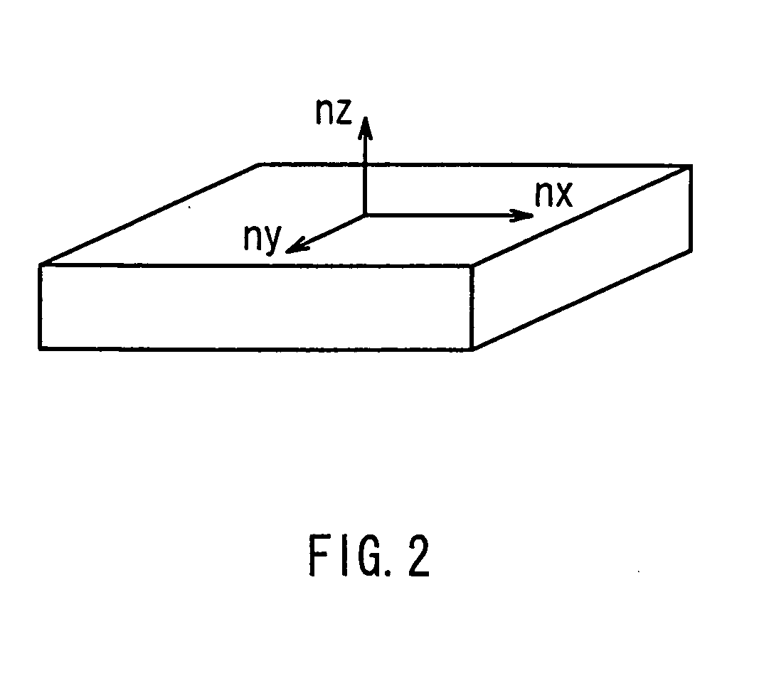
First, 90 parts by weight of a nematic liquid crystal monomer represented by the chemical formula (10) below, 10 parts by weight of a polymerizable chiral dopant having a helical twisting power of 5.5×10⁻⁴ nm−1.(wt %)−1 represented by the formula (38) below, 5 parts by weight of a UV polymerization initiator (trade name: IRGACURE 907; manufactured by Ciba Specialty Chemicals, used also in the following examples) and 300 parts by weight of methyl ethyl ketone were mixed. Then, this mixture was applied onto an alignment substrate (a polyester film with a thickness of 75 μm). Thereafter, this mixture was subjected to a heat treatment at 70° C. for 3 minutes, thereby aligning the monomer. Subsequently, the monomer was polymerized by an ultraviolet irradiation so as to fix the orientation. Then, the alignment substrate was removed, thus obtaining a completely transparent and smooth retardation film having a thickness of about 2 μm. This retardation film was a birefringent layer of nx≈ny>nz and had a selective reflection wavelength range of 200 to 220 nm.

Example

Example 2
In a manner similar to that in Example 1, 92 parts by weight of the nematic liquid crystal monomer represented by the chemical formula (10) above, 8 parts by weight of the polymerizable chiral dopant having a helical twisting power of 5.5×10⁻⁴ nm−1.(wt %)−1 represented by the chemical formula (38) above, 5 parts by weight of the UV polymerization initiator and 300 parts by weight of methyl ethyl ketone were mixed. Then, this mixture was applied onto an alignment substrate (a polyester film with a thickness of 75 μm). Thereafter, this mixture was subjected to a heat treatment at 80° C. for 3 minutes, thereby aligning the monomer. Subsequently, the monomer was polymerized by an ultraviolet irradiation so as to fix the orientation. Then, the alignment substrate was removed, thus obtaining a completely transparent and smooth retardation film having a thickness of about 2 μm. This retardation film was a birefringent layer of nx≈ny>nz and had a selective reflection wavelength range of 290 to 310 nm.

Example

Example 3
In a manner similar to that in Example 1, 91 parts by weight of the nematic liquid crystal monomer represented by the chemical formula (10) above, 9 parts by weight of the polymerizable chiral dopant having a helical twisting power of 5.5×10⁻⁴ nm−1.(wt %)−1 represented by the formula (38) above, 5 parts by weight of the UV polymerization initiator and 300 parts by weight of methyl ethyl ketone were mixed. Then, this mixture was applied onto an alignment substrate (a polyester film with a thickness of 75 μm). Thereafter, this mixture was subjected to a heat treatment at 80° C. for 3 minutes, thereby aligning the monomer. Subsequently, the monomer was polymerized by an ultraviolet irradiation so as to fix the orientation. Then, the alignment substrate was removed, thus obtaining a completely transparent and smooth retardation film having a thickness of about 2 μm. This retardation film was a birefringent layer of nx≈ny>nz and had a selective reflection wavelength range of 240 to 260 nm.

PUM

no PUM

Description & Claims & Application Information

We can also present the details of the Description, Claims and Application information to help users get a comprehensive understanding of the technical details of the patent, such as background art, summary of invention, brief description of drawings, description of embodiments, and other original content. On the other hand, users can also determine the specific scope of protection of the technology through the list of claims; as well as understand the changes in the life cycle of the technology with the presentation of the patent timeline. Login to view more.

Similar technology patents

Liquid crystal display device

InactiveUS20060215093A1excellent display qualityincrease viewing angle
Owner:JAPAN DISPLAY CENT INC

Particles for display media and information display panel using the particles

InactiveUS20070236776A1excellent display quality
Owner:BRIDGESTONE CORP

Display device

ActiveUS20070040981A1excellent display quality
Owner:TRIVALE TECH

Wavelength conversion device, laser apparatus, image forming apparatus, and display apparatus

InactiveUS20100073755A1excellent display quality
Owner:RICOH KK

Classification and recommendation of technical efficacy words

  • suppress light leakage
  • excellent display quality

Liquid crystal display device

ActiveUS20090079921A1high precisionsuppress light leakage
Owner:NEC LCD TECH CORP

Acrylic resin composition

InactiveUS20050244657A1improve durabilitysuppress light leakage
Owner:SUMITOMO CHEM CO LTD

FFS mode liquid crystal display panel

ActiveUS20070229749A1wide view angleexcellent display quality
Owner:JAPAN DISPLAY WEST

Optical multilayer film and image display device

ActiveUS20080180801A1excellent display qualityprevent occurrence
Owner:FUJIFILM CORP

Liquid crystal display device

ActiveUS20070211187A1high brightnessexcellent display quality
Owner:SHARP KK

Light emitting device and electronic apparatus

ActiveUS20140027792A1high luminanceexcellent display quality
Owner:SEIKO EPSON CORP
Why Eureka
Try Eureka