Tantalum barrier layer for copper metallization

a technology of copper metallization and barrier layer, which is applied in the direction of basic electric elements, semiconductor/solid-state device manufacturing, electric apparatus, etc., can solve the problem of process deleteriously and remove the barrier

a technology of copper metallization and barrier layer, which is applied in the direction of basic electric elements, semiconductor/solid-state device manufacturing, electric apparatus, etc., can solve the problem of process deleteriously and remove the barrier

US20050074968A1Inactive Publication Date: 2005-04-07APPLIED MATERIALS INC

Image

  • Tantalum barrier layer for copper metallization
  • Tantalum barrier layer for copper metallization
  • Tantalum barrier layer for copper metallization

Examples


Embodiment Construction

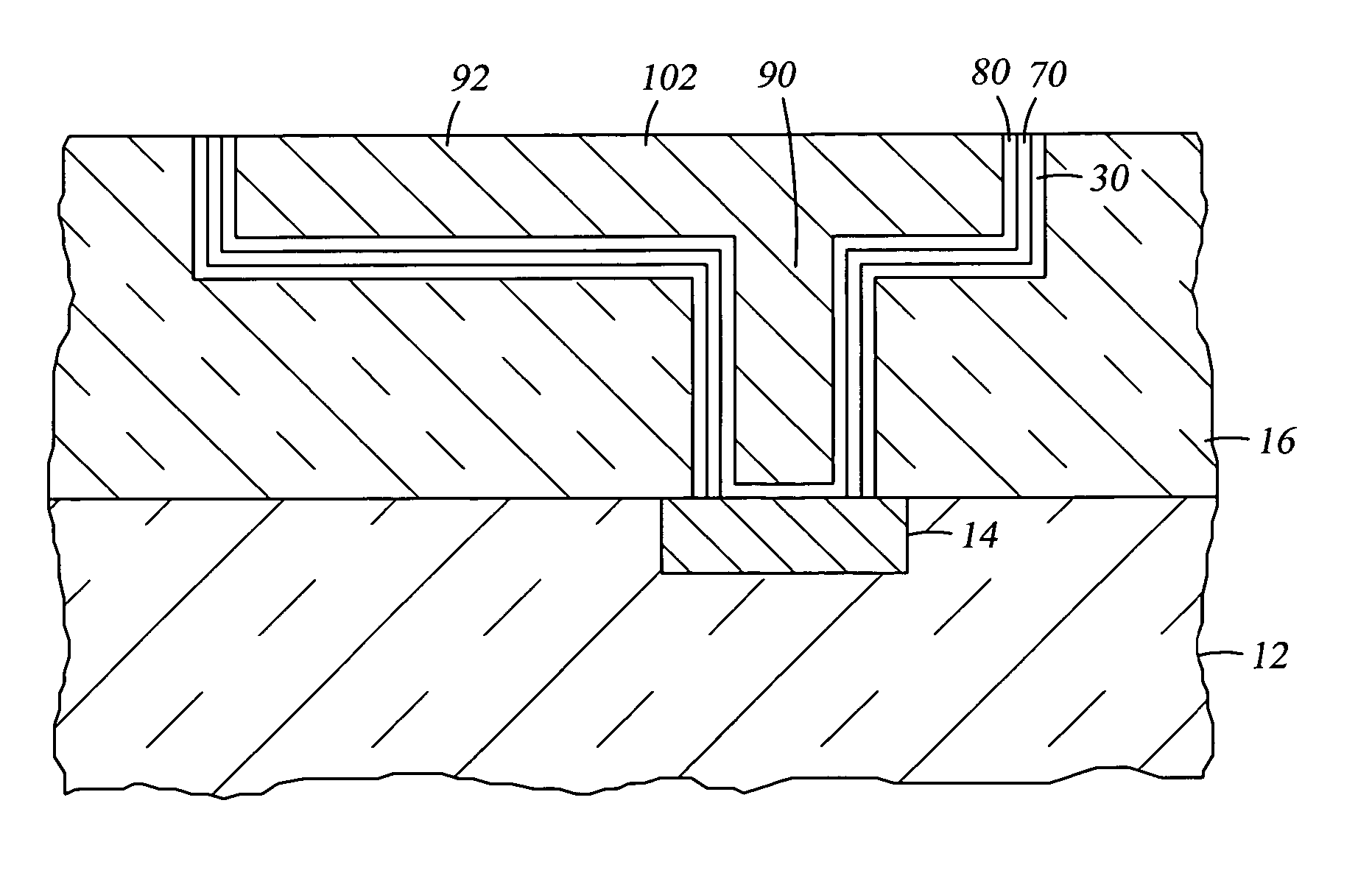
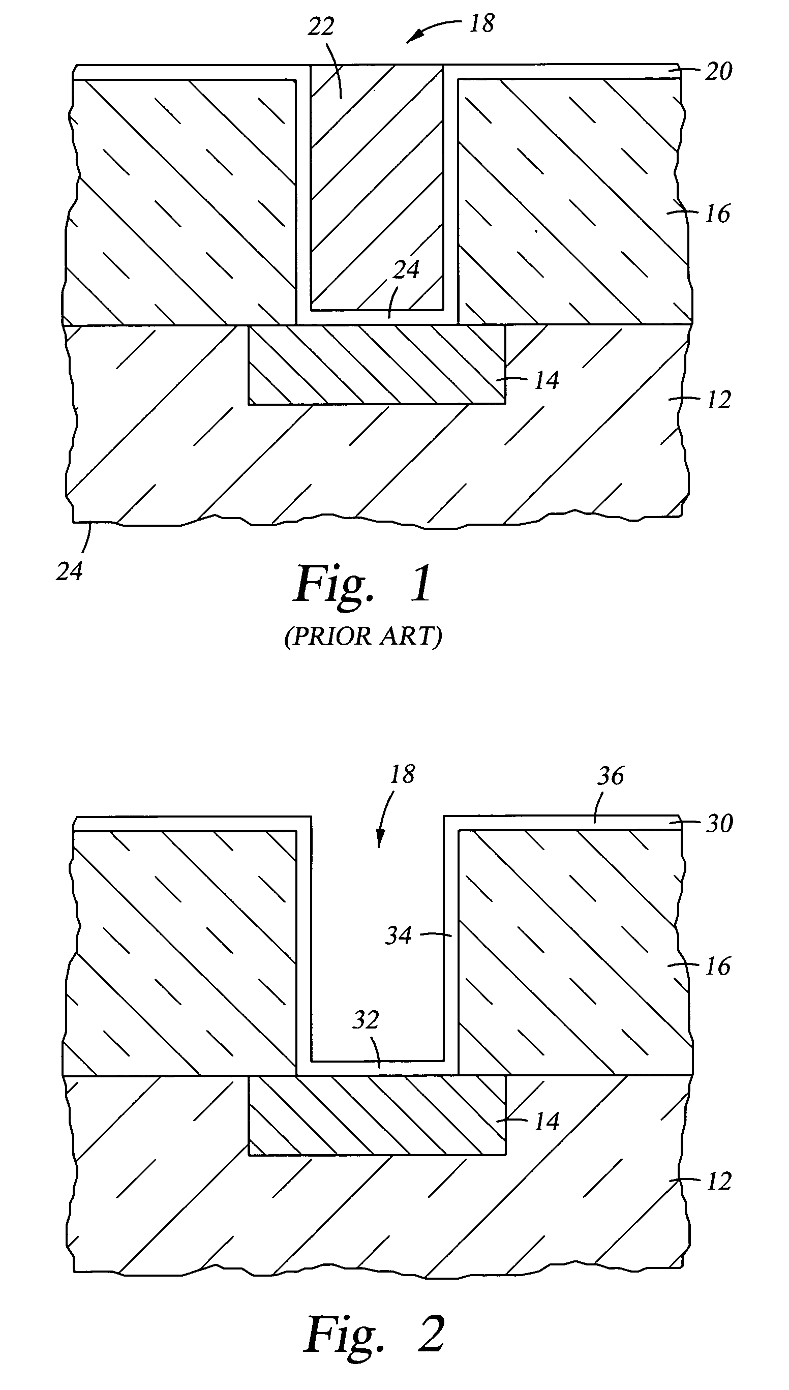
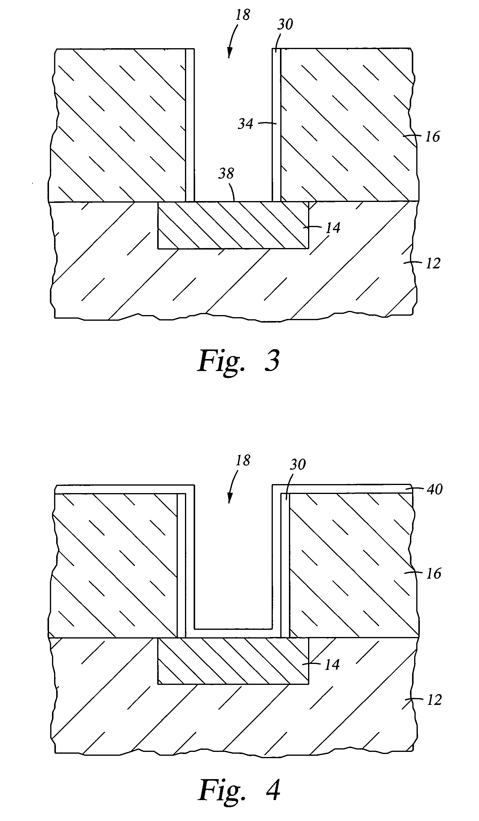
It is has been found useful to form a via barrier in two chambers. The first step is performed in a CVD (chemical vapor deposition) chamber in which a CVD barrier layer 30, as illustrated in the cross-sectional view of FIG. 2, is first deposited having a composition of titanium silicon nitride (TiSiN). Again, the illustrated structure ignores features such as etch stop layers and dual-damascene holes. The CVD barrier layer 30 may be formed by a three-step process in the T×Z plasma CVD reactor, available from Applied Materials, Inc. of Santa Clara, Calif. Zhao et al. describe a version of this chamber and a TiN deposition procedure in U.S. Pat. No. 5,846,332. In the first step, a TiN layer is deposited to a thickness of about 5 nm by a well known process of thermal chemical vapor deposition at about 350° C. using tetrakis-dimethyl-amido titanium (TDMAT) as the precursor gas. Koai et al. describe an alternative plasma CVD process and chamber in U.S. Pat. No. 6,106,625. The thermal CV...


PUM


Abstract

A method of forming barrier layers in a via hole extending through an inter-level dielectric layer and including a preformed first barrier coated onto the bottom and sidewalls of the via holes. In a single plasma sputter reactor, a first step sputters the wafer rather than the target with high energy ions to remove the barrier layer from the bottom of the via but not from the sidewalls and a second step sputter deposits a second barrier layer, for example of Ta / TaN, onto the via bottom and sidewalls. The two steps may be differentiated by power applied to the target, by chamber pressure, or by wafer bias. The second step may include the simultaneous removal of the first barrier layer from the via bottom and sputter deposition of the second barrier layer onto the via sidewalls.

Description

FIELD OF THE INVENTION The invention relates generally to processes for formation of vertical interconnects in integrated circuits. In particular, the invention relates to a tantalum barrier layer for copper metallization. BACKGROUND ART Modern integrated circuits include several levels of metallization formed over the active semiconductor circuitry formed in the substrate, most commonly a silicon wafer. The multiple metallization layers are required to interconnect the millions to tens of millions of discrete semiconductor devices formed in a single integrated circuit. For advanced microprocessors, there may be five or more levels of metallization. Each metallization layer includes a dielectric layer, for example, of silicon dioxide or possibly a low-k dielectric material deposited over the previous layer, a via (or contact) hole etched through the dielectric layer, and a metallization including a vertical metallic plug filled into the hole and a horizontal interconnect formed o...

Claims


Application Information

Patent Timeline
07 Apr 2005
Publication
US20050074968A1
IPC
H01L21/285; H01L21/4763; H01L21/768
CPC
H01L21/2855; H01L21/28556; H01L21/76843; H01L21/76865; H01L21/76846; H01L21/76856; H01L21/76844
Inventors
CHEN, LING; GANGULI, SESHADRI