Semiconductor device having heat radiation plate and bonding member

a technology of heat radiation plate and bonding member, which is applied in the direction of semiconductor devices, semiconductor/solid-state device details, electrical apparatus, etc., can solve the problems of not substantially reducing the performance of heat radiation, and achieve the effects of preventing cracking, high reliability of bonding member, and improving strength of bonding member

Active Publication Date: 2005-04-14
DENSO CORP
View PDF7 Cites 29 Cited by
  • Summary
  • Abstract
  • Description
  • Claims
  • Application Information

AI Technical Summary

Benefits of technology

[0017] Further, a semiconductor device includes a heat generation element; a bonding member; first and second heat radiation plates disposed on first and second sides of the heat generation element through the bonding member; and a resin mold molding almost all of the device. The first and second heat radiation plates are capable of radiating heat generated from the heat generation element. The heat generation element electrically and thermally connects to the first and second heat radiation plates through the bonding member. The resi

Problems solved by technology

Further, even if the crack is generated in the bonding member, the crack does not affect th

Method used


Image

  • Semiconductor device having heat radiation plate and bonding member
  • Semiconductor device having heat radiation plate and bonding member
  • Semiconductor device having heat radiation plate and bonding member

Examples


first embodiment

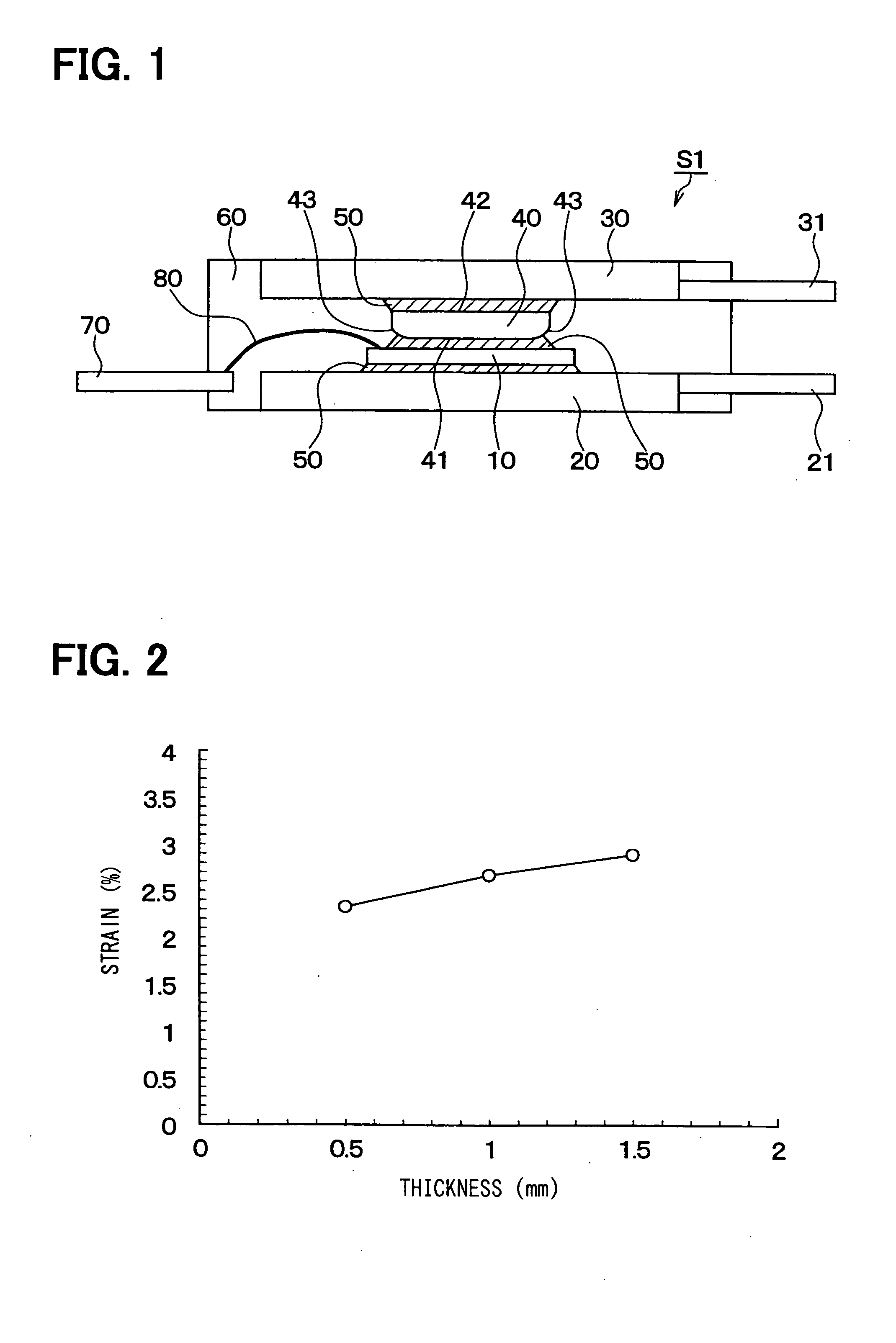
[0036] The inventors have studied about a heat radiation block (i.e., a heat sink block) in a semiconductor device. This is because dimensions and shape of the heat radiation block may affect a distortion at a bonding portion between the heat radiation block and a solder layer. Specifically, the distortion is analyzed by a finite element method (i.e., FEM). As a result, for example, when the heat radiation block is thick, a bonding member disposed between a heat generation element, i.e., a semiconductor chip and the heat radiation block becomes distorted largely. In this case, the bonding member may crack by a heat cycle stress. The detailed description is described as follows.

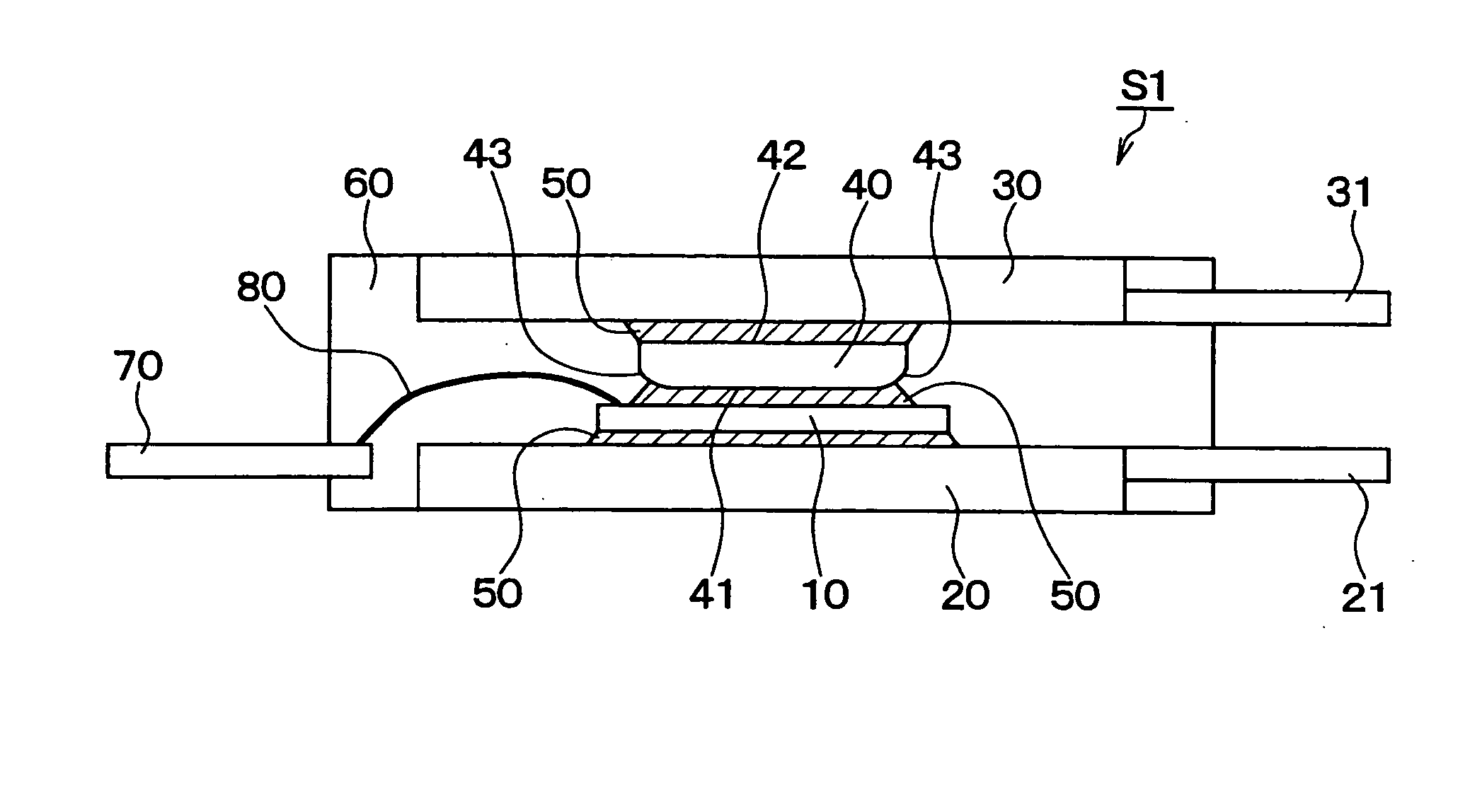
[0037]FIG. 1 shows a semiconductor device S1 according to a first embodiment of the present invention. The device S1 includes a semiconductor chip 10 as a heat generation element, upper and lower heat sinks 20, 30 as a heat radiation plate, a heat sink block 40 as a heat radiation block, a bonding member 50 d...

second embodiment

[0067] A semiconductor device S2 according to a second embodiment of the present invention is shown in FIG. 5. The bottom 41 of the heat sink block 40 disposed on the chip side is rounded. Specifically, whole bottom surface 41 of the heat sink block 40 is formed to be a spherical surface. Here, at least one of the top 42 and the bottom 41 of the heat sink block 40 can be the spherical surface. The top 42 of the heat sink block 40 is disposed on the upper heat sink side.

[0068] In FIG. 5, the bottom 41 of the heat sink block 40 disposed on the semiconductor chip side is formed into the spherical shape. However, the top 42 of the heat sink block 40 disposed on the upper heat sink side can be formed into the spherical shape. Further, both of the bottom 41 and the top 42 of the heat sink block 40 can be formed into the spherical shape. Here, the device S2 has the heat sink block 40 with the thickness in a range between 0.5 mm and 1.5 mm.

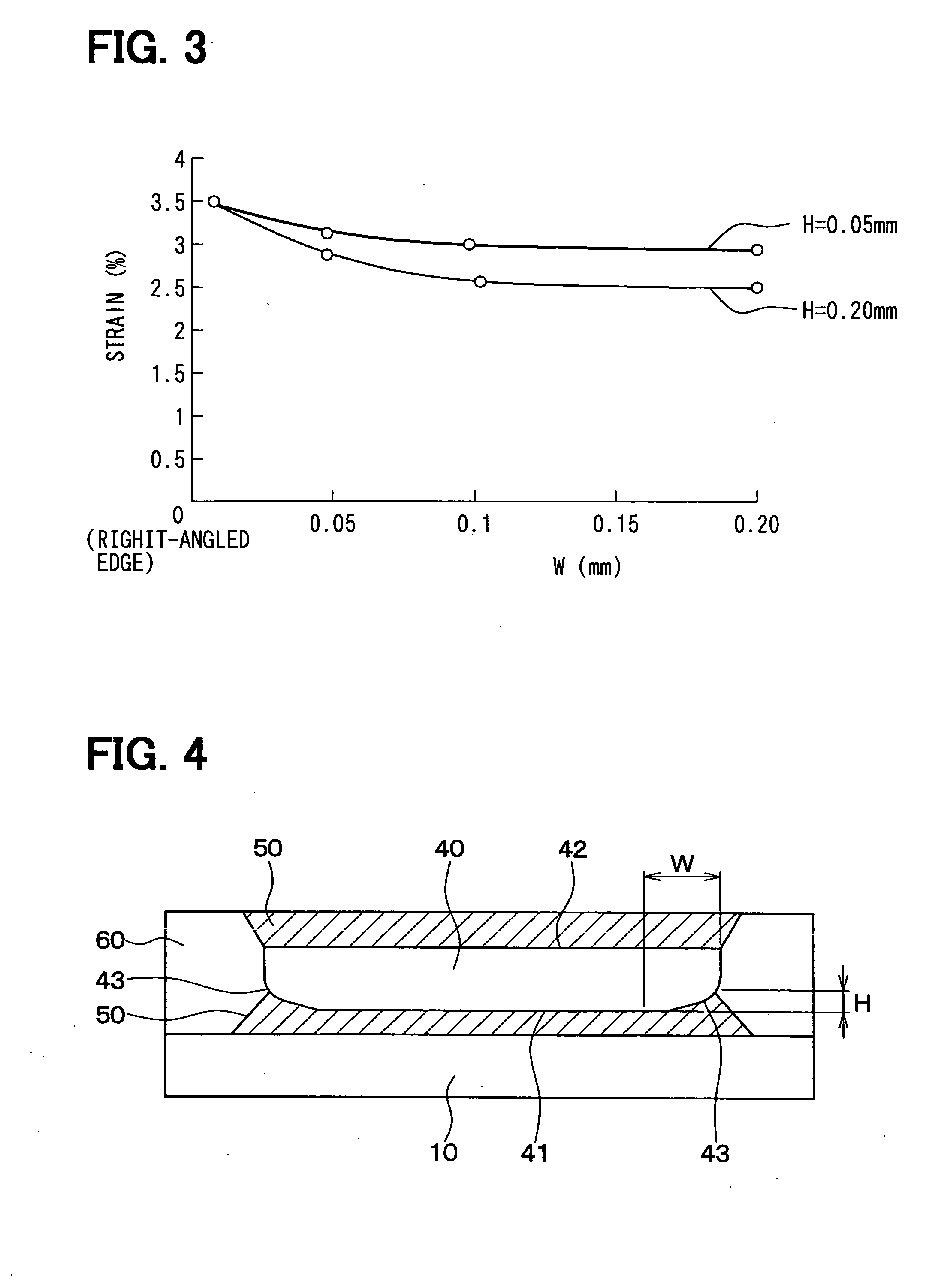
[0069] The width W of the edge portion 43 of the ...

third embodiment

[0073] A semiconductor device S3 according to a third embodiment of the present invention is shown in FIG. 7. The semiconductor chip 10 has an edge portion 11, which is rounded so that the bonding member 50 contacting the chip 10 becomes thicker. Specifically, the edge 11 of the chip 10 is formed into a R-shape so that the bonding member 50 disposed at the edge portion 11 of the chip 10 and disposed between the chip 10 and the lower heat sink 20 becomes thicker.

[0074] In FIG. 7, the device S3 has the heat sink block 40 with the rounded edge portion 43 thereof. However, the device S3 can have the heat sink block 40 having the spherical shaped bottom 41 thereof.

[0075] In this case, the device S3 has the same advantages (i.e., functions and effects) as the device S1 having the edge portion 43 of the heat sink block 40 formed into the rounded edge.

[0076] According to the FEM analysis, the stress in the bonding member 50 disposed between the chip 10 and the lower heat sink 20 is conce...


PUM


Abstract

A semiconductor device includes a heat generation element; a bonding member; first and second heat radiation plates disposed on first and second sides of the heat generation element through the bonding member; a heat radiation block disposed between the first heat radiation plate and the heat generation element through the bonding member; and a resin mold. The heat radiation block has a thickness in a range between 0.5 mm and 1.5 mm. The semiconductor device has high reliability of the bonding member.

Description

CROSS REFERENCE TO RELATED APPLICATIONS [0001] This application is based on Japanese Patent Applications No. 2003-350814 filed on Oct. 9, 2003, No. 2003-352513 filed on October 10, and No. 2003-395572 filed on Nov. 26, 2003, the disclosures of which are incorporated herein by reference. FIELD OF THE INVENTION [0002] The present invention relates to a semiconductor device having a heat radiation plate and a bonding member. BACKGROUND OF THE INVENTION [0003] A semiconductor chip having high withstand voltage and large current capacity generates large heat while operating. Therefore, it is required to improve heat radiation radiated from the chip. In view of the heat radiation, a semiconductor device having a large current semiconductor chip is disclosed in Japanese Patent Application Publication No. 2003-110064 (i.e., U.S. patent application Publication No. 2003-0022464-1l). The semiconductor device includes a pair of heat sinks made of metal, which are disposed on both sides of the s...

Claims


Application Information

Patent Timeline
IPC IPC(8): H01L21/60H01L23/00H01L23/36H01L23/42H01L23/433H01L23/492H01L23/58
CPCH01L23/4334H01L23/492H01L23/562H01L24/32H01L24/33H01L24/45H01L24/83H01L2224/29111H01L2224/32245H01L2224/45124H01L2224/45144H01L2224/48091H01L2224/48247H01L2224/73215H01L2224/73265H01L2224/83801H01L2924/01005H01L2924/01013H01L2924/01014H01L2924/01029H01L2924/0105H01L2924/01074H01L2924/01079H01L2924/01082H01L2924/13055H01L2924/18301H01L2924/19043H01L24/48H01L2224/2919H01L2924/01006H01L2924/01033H01L2924/01068H01L2924/014H01L2924/0665H01L2924/0134H01L2924/15724H01L2924/15747H01L2224/29299H01L2224/2929H01L2924/00013H01L2924/01028H01L2924/1301H01L2924/1305H01L2924/00014H01L2924/00H01L2924/3512H01L2924/01051H01L2924/00012H01L2224/29099H01L2224/29199H01L24/73H01L2224/2612H01L2924/181H01L2924/351
Inventor HIRANO, NAOHIKOKATO, NOBUYUKIMAMITSU, KUNIAKINAKASE, YOSHIMI
Owner DENSO CORP
Why Eureka
Try Eureka