Integrated circuit

a technology of integrated circuits and resistors, applied in the field of integrated circuits, can solve the problems of inability to adapt to the changing state of the integrated circuit, requiring the use of dedicated external resistors for maintaining the transconductance constant, and requiring one or more extra pins on the integrated circui

Inactive Publication Date: 2005-04-14
TELEFON AB LM ERICSSON (PUBL)
View PDF13 Cites 1 Cited by
  • Summary
  • Abstract
  • Description
  • Claims
  • Application Information

AI Technical Summary

Benefits of technology

[0016] The invention has the advantage that it does not require the use of an external frequency reference, an extra external resistor or any extra external pins.

Problems solved by technology

This variation is unacceptable for integrated circuits which rely on a constant transconductance.
U.S. Pat. No. 4,388,539 discloses a constant Gm circuit which, as above, has the disadvantage of requiring the use of a dedicated external resistor for maintaining the transconductance constant.
Thus, all of the known solutions have the disadvantage of requiring an extra external frequency reference or a dedicated external resistor to achieve a constant transconductance, the external frequency reference or resistor being used to fine tune the filter response.
The need for an external frequency reference or resistor also has the disadvantage of requiring one or more extra pins on the integrated circuit.

Method used


Image

  • Integrated circuit
  • Integrated circuit
  • Integrated circuit

Examples


Embodiment Construction

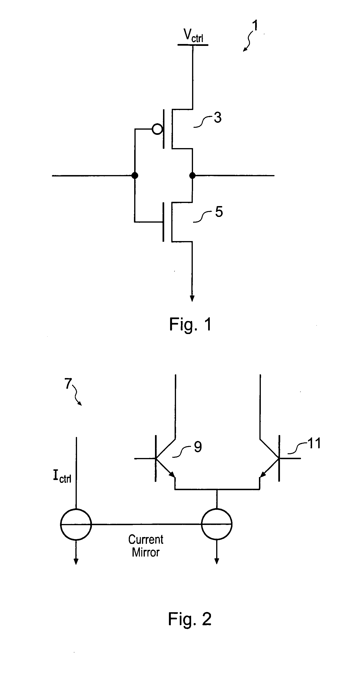
[0027]FIG. 1 shows a typical Gm cell 1, namely a CMOS inverter comprising first and second transistors 3, 5. The transconductance of such a Gm cell 1 is controlled by controlling the total voltage Vctrl applied across the Gm cell 1.

[0028]FIG. 2 shows another common type of Gm cell 7, namely a bipolar differential pair configuration comprising transistors 9, 11. The transconductance of the bipolar differential pair configuration 7 is controlled by controlling the bias current Ictrl.

[0029] Reference will now be made to how the transconductance of a Gm cell, for example a Gm-cell 1, 7 as shown in FIG. 1 or 2, is maintained constant in accordance with the invention. It is noted that FIGS. 1 and 2 give examples of transconductance amplifiers in their simplest forms, and the invention can be applied to any transconductance circuit arrangement, which has means of controlling its transconductance by means of a control voltage or control current.

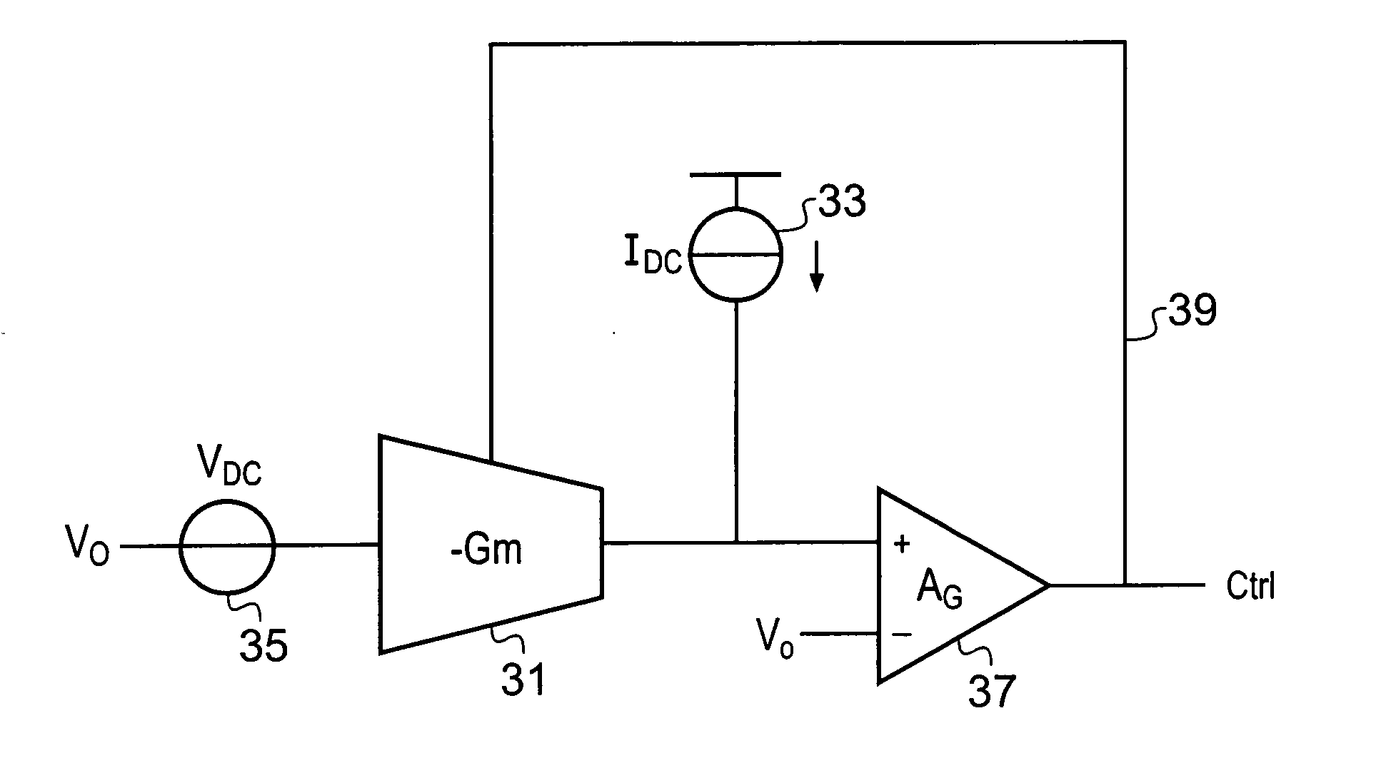
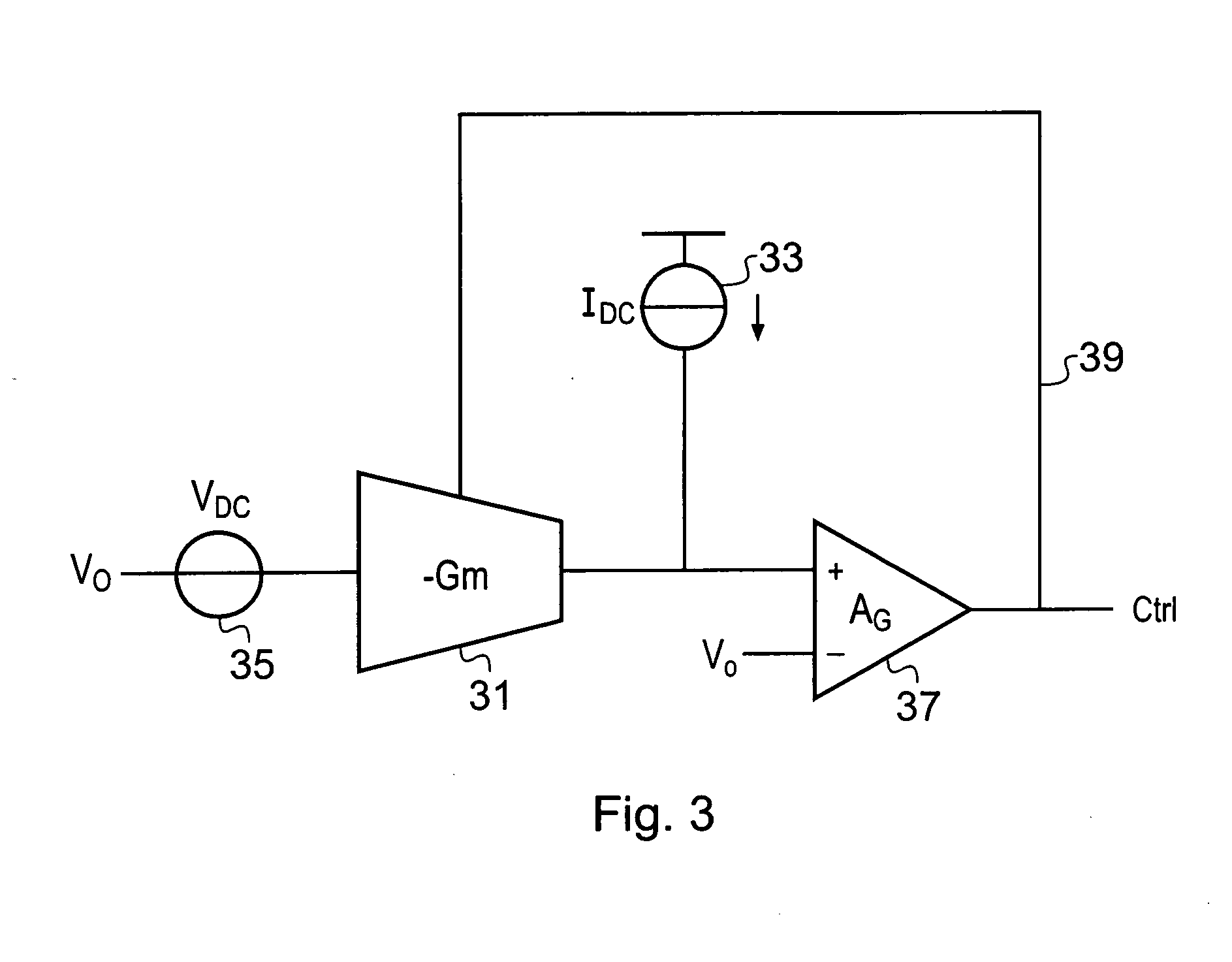
[0030]FIG. 3 shows a block diagram of a cir...


PUM


Abstract

An integrated circuit comprises a biasing circuit for maintaining the transconductance of a Gm cell constant. The integrated circuit comprises an on-chip constant voltage source and an on-chip constant current source. The on-chip constant current source has a connection for an external resistance, the value of the external resistance determining the current generated by the constant current source. The biasing circuit comprises means for providing a first fraction (β) of the current generated by the on-chip current source to bias the output of the Gm cell, and means for providing a second fraction (α) of the voltage generated by the on-chip voltage source to bias the input of the Gm cell. The transconductance of the Gm cell is controlled to be equal to the ratio of said fraction of the current generated by the on-chip current source to said fraction of the voltage generated by the on-chip voltage source.

Description

FIELD OF THE INVENTION [0001] The invention relates to an integrated circuit, and in particular, to an integrated circuit having a biasing circuit for maintaining the transconductance of a Gm cell constant. BACKGROUND OF THE INVENTION [0002] The transconductance (Gm) of a cell is defined as the ratio of the output current IOUT to the input voltage VIN. The transconductance of a Gm cell on an integrated circuit varies over process and temperature. Depending on the on-chip components used for the cell, this variation can be greater than ±30%. [0003] This variation is unacceptable for integrated circuits which rely on a constant transconductance. For example, a constant transconductance is required in order to keep the gain constant in low noise amplifiers (LNAs) having inductive collector loads, or to minimise the variation in the start up gain of a voltage controlled oscillator (VCO). In another example, a constant transconductance is required to minimise frequency error in a constan...

Claims


Application Information

Patent Timeline
Patent Type & Authority Applications(United States)
IPC IPC(8): H03F3/68H03H11/54
CPCH03H11/54H03F3/68
Inventor MATTSSON, ULFWILSON, GORDON
Owner TELEFON AB LM ERICSSON (PUBL)
Why Eureka
Try Eureka