Light-emitting device and method of manufacturing the same

a technology of light-emitting devices and manufacturing methods, which is applied in the direction of solid-state devices, lasers, semiconductor lasers, etc., can solve the problems of void formation in the lower portion, decreased light extraction efficiency, and increased manufacturing process and cost, and achieves the effect of high light extraction efficiency

Inactive Publication Date: 2005-04-21
SAMSUNG ELECTRO MECHANICS CO LTD
View PDF5 Cites 75 Cited by
  • Summary
  • Abstract
  • Description
  • Claims
  • Application Information

AI Technical Summary

Benefits of technology

[0014] The present invention provides a light-emitting device and a method of manufacturing the same. The light-emitting device includes a substrate having at least one protruded portion with a curved surface in which a consistent defect density and uniform stress distribution can be obtained even when the growth of the semiconductor crystal layer and the forming of the light-emitting device are completed. In addition, the light-emitting device has a high the light extraction efficiency for extracting light generated at a electroluminescense layer externally.

Problems solved by technology

In a general LED, the most important issue is how efficiently can the light, which is created at an internal active layer, be extracted externally.
Therefore to extract the light in a longitudinal direction, various methods such as forming the side walls of the structure of accumulative layers of a semiconductor device to have a predetermined angle, and forming side walls composed of reflective material have been made, but this caused problems in the manufacturing process and increased costs.
This process has a disadvantage in that when growing the semiconductor crystal layer using such a patterned sapphire substrate (PSS), since planarization is carried out after facet growth is performed on the pattern, regrowth has to be done to a sufficient thickness to perform planarization.
However, a disadvantage is that a void is formed in the lower portion of the step difference and to planarize the growth layer group III nitride compound semiconductors have to be formed relatively thick.
However, in the case of the ELOG method a separate mask layer is needed, and in the case of the PENDEO method, a void is formed on the interface portion of the substrate resulting in a decrease in light extraction efficiency.

Method used


Image

  • Light-emitting device and method of manufacturing the same
  • Light-emitting device and method of manufacturing the same
  • Light-emitting device and method of manufacturing the same

Examples


Embodiment Construction

[0034] The above and other features and advantages of the present invention will become more apparent by describing in detail exemplary embodiments thereof with reference to the attached drawings.

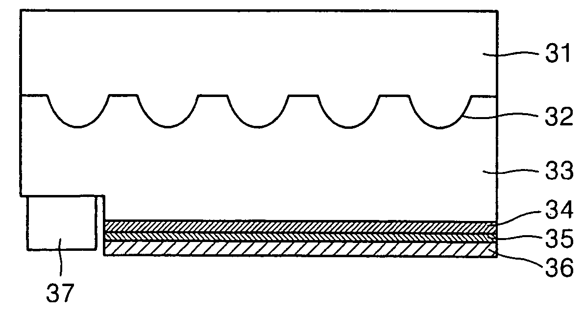
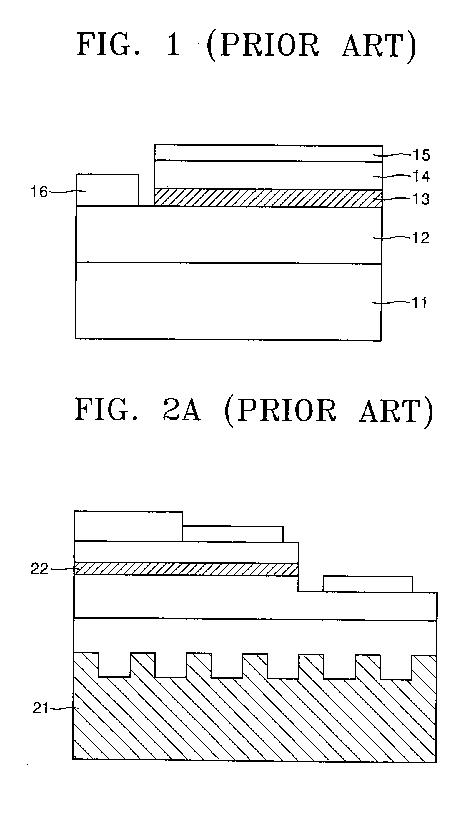
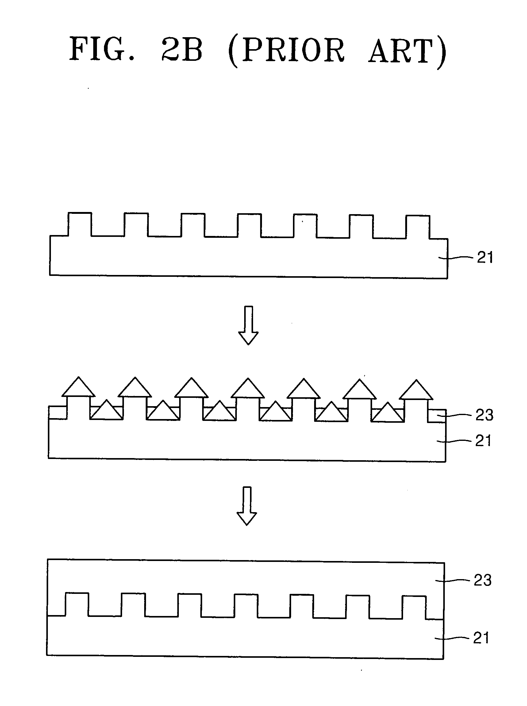
[0035]FIG. 3a is a cross-sectional view of a substrate of a light-emitting device which might include sapphire or Si according to an embodiment of the present invention. As shown in FIG. 3a, smoothly curved protrusions 32 are formed on the surface of a substrate 31. Such protrusions 32 are different from the uneven structure of the general substrate shown in FIGS. 2a through 2c. In other words, the top portion and side portion of the uneven structure of FIGS. 2a through 2c are discriminated since the top portion and side portion are each flat and the side portions are slanted at a predetermined angle with respect to the surface of the substrate 21.

[0036] However, the protruded portions 32 formed on the surface of the substrate of FIG. 3a has a curved surface, and thus there is not distinc...


PUM


Abstract

Provided is a light-emitting device and a method of manufacturing the same. The light-emitting device includes a substrate having at least one protruded portion with a curved surface in which a consistent defect density and uniform stress distribution can be obtained even when the growth of the semiconductor crystal layer and the forming of the light-emitting device are completed. In addition, the light-emitting device has a high the light extraction efficiency for extracting light generated at an electroluminescense layer externally.

Description

BACKGROUND OF THE INVENTION [0001] This application claims the priority of Korean Patent Application No. 2003-73442 filed on Oct. 21, 2003, in the Korean Intellectual Property Office, the disclosure of which is incorporated herein in its entirety by reference. [0002] 1. Field of the Invention [0003] The present invention relates to a light-emitting device, and more particularly, to a high efficiency light-emitting device with improved light extraction efficiency and good defect density control and stress distribution control and, in which, a substrate limits a surface crystal orientation. [0004] 2. Description of the Related Art [0005] In general, light-emitting devices include laser diodes (LD) and light emitting diodes (LED), and LEDs use properties of compound semiconductors to transmit a signal, which is electric energy converted into an infra-red light, visible light, or other forms of light. The converting of electric energy into light can be categorized into temperature radia...

Claims


Application Information

Patent Timeline
Patent Type & Authority Applications(United States)
IPC IPC(8): H01L27/15H01L33/32H01S5/00
CPCH01L33/22H01L33/12
Inventor LEE, JEONG-WOOKSUNG, YOUN-JOONCHO, JAE-HEEPAEK, HO-SUN
Owner SAMSUNG ELECTRO MECHANICS CO LTD
Why Eureka
Try Eureka