Semiconductor device using insulating film of low dielectric constant as interlayer insulating film
- Summary
- Abstract
- Description
- Claims
- Application Information
AI Technical Summary
Benefits of technology
Problems solved by technology
Method used
Image

Examples
first embodiment
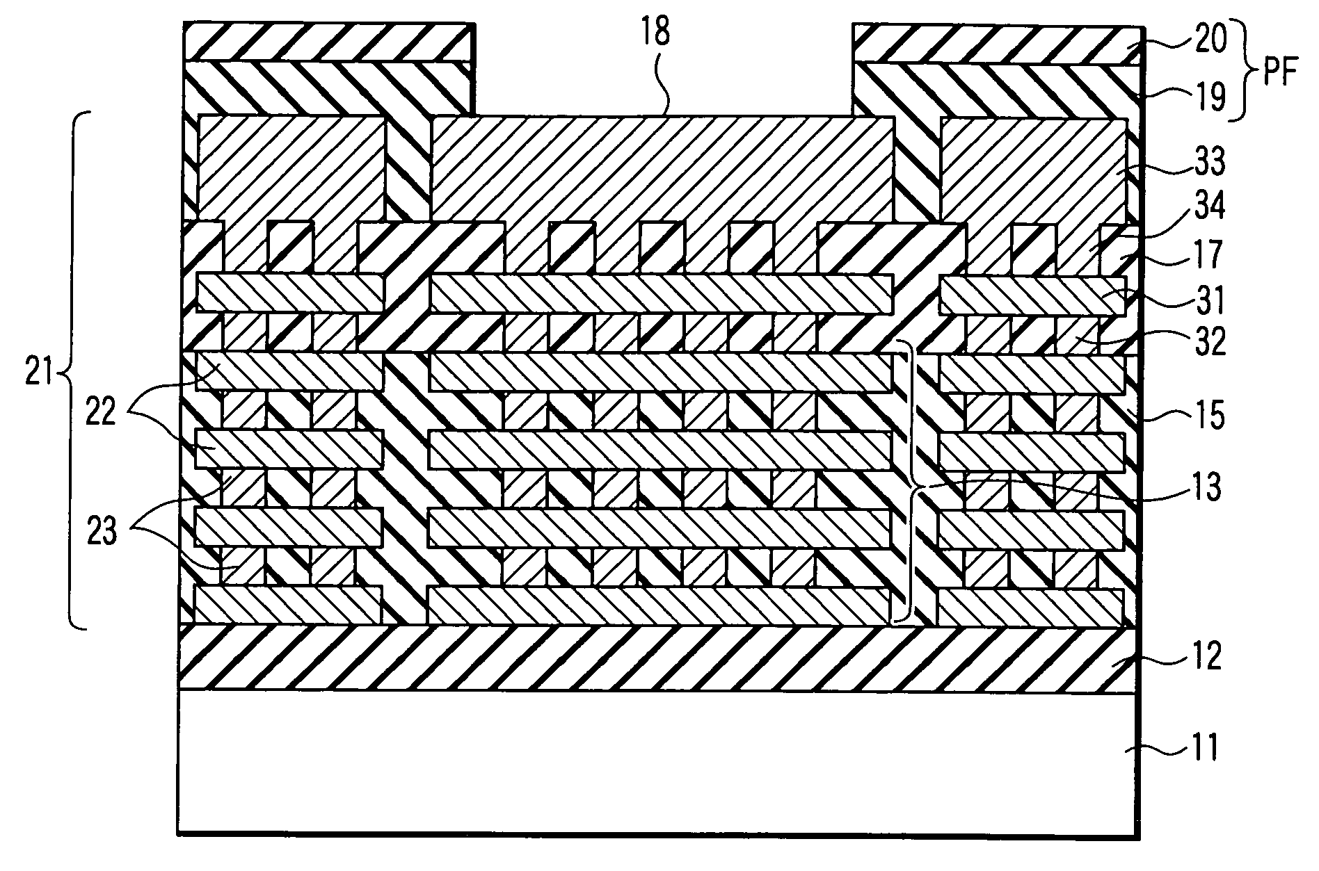
[0037]FIGS. 1 and 2 show a semiconductor device according to a first embodiment of the present invention. As shown in FIGS. 1 and 2, a ring-like continuous dummy multilevel interconnection configuration 21 is disposed in an insulating film 15 of low dielectric constant formed around the periphery of an electrode pad 18. The dummy multilevel interconnection configuration comprises a plurality of interconnection layers 22 corresponding in number to the layers of the multilevel interconnection configuration below the pad and a plurality of vias 23 that interconnect the interconnection layers 22.
[0038] That is, in FIG. 2, a semiconductor substrate 11 in which, though not shown, devices, such as transistors, have been formed is formed on top with an insulating film 12. For example, four levels of interconnections 13 are formed as the multilevel interconnection configuration on the insulating film 12. The interconnection layers 13 are interconnected by vias 14. The interconnection layers...
second embodiment
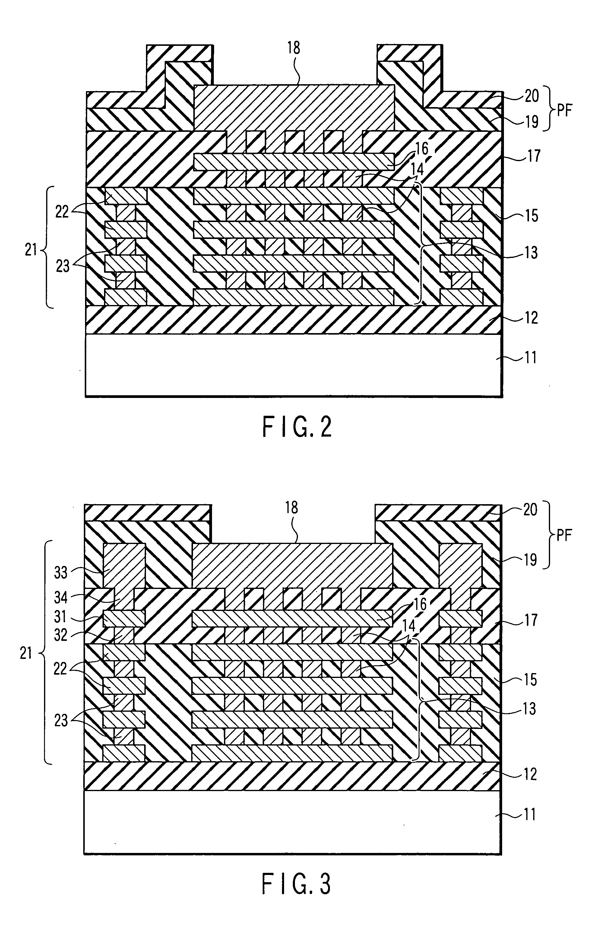
[0048]FIG. 3 shows a second embodiment of the present invention. In the first embodiment, the dummy multilevel interconnection configuration 21 is formed only within the insulating film 15 of low dielectric constant. Unlike the first embodiment, in the second embodiment, the dummy multilevel interconnection configuration 21 is formed within both the insulating film 17 on the insulating film 15 of low dielectric constant and the silicon oxide film 19.
[0049] That is, as shown in FIG. 3, an interconnection layer 31 and its associated vias 32 as well as an interconnection layer 16 and its associated vias 14 are formed within the insulating film 17 and an interconnection layer 33 is formed within the silicon oxide film 19. The interconnection layer 33 is connected to the underlying interconnection layer 31 through vias 34.
[0050] According to the second embodiment, the dummy multilevel interconnection configuration 21 is also formed within the insulating film 17 and the silicon oxide fi...
third embodiment
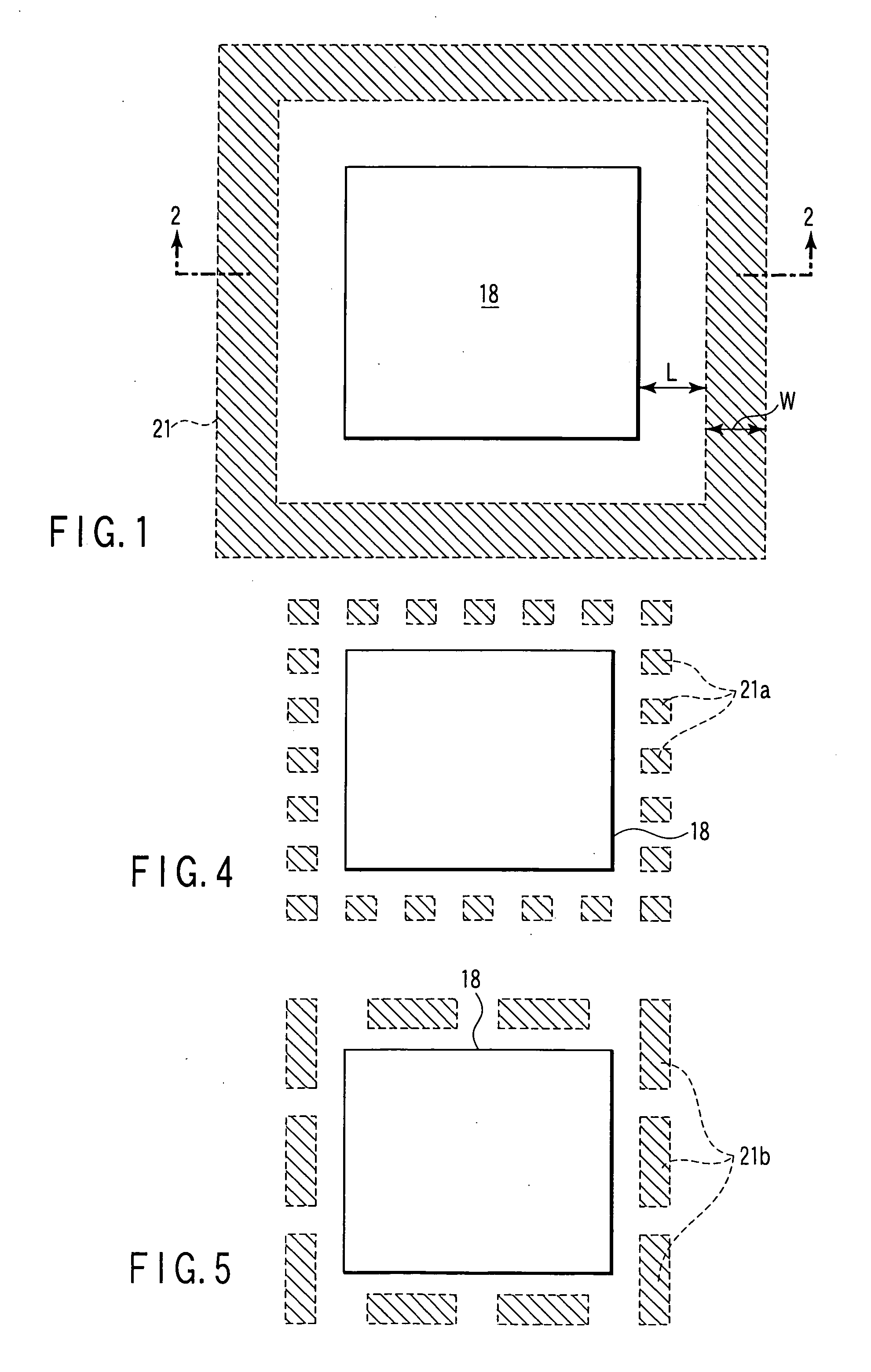
[0051]FIGS. 4 and 5 show a third embodiment of the present invention. In the first and second embodiments, the dummy multilevel interconnection configuration 21 is formed around the electrode pad 18 in the shape of a continuous ring so as to completely surround the multilevel interconnection configuration 13. Unlike the first and second embodiments, in the third embodiment, the dummy multilevel interconnection configuration 21 is divided into interconnection patterns which are, for example, square or rectangular in plane shape. That is, FIG. 4 shows a configuration such that square-shaped dummy multilevel interconnection patterns 21a are arranged around the electrode pad 18 at regular intervals. FIG. 5 shows a configuration such that rectangular-shaped dummy multilevel interconnection patterns 21b are arranged around the electrode pad 18 at regular intervals.
[0052] The third embodiment can also provide substantially the same advantage as the first and second embodiments.
PUM
 Abstract
Description
Claims
Application Information
 - Generate Ideas
- Intellectual Property
- Life Sciences
- Materials
- Tech Scout
- Unparalleled Data Quality
- Higher Quality Content
- 60% Fewer Hallucinations
Browse by: Latest US Patents, China's latest patents, Technical Efficacy Thesaurus, Application Domain, Technology Topic, Popular Technical Reports.
© 2025 PatSnap. All rights reserved.Legal|Privacy policy|Modern Slavery Act Transparency Statement|Sitemap|About US| Contact US: help@patsnap.com