Display device

a display device and display technology, applied in the field of display devices, can solve the problems of increasing manufacturing man-hours and thus being unfavorable, and achieve the effects of imparting flexibility, imparting flexibility, and imparting flexibility to the formation of wiring layers

Active Publication Date: 2005-04-21
SAMSUNG DISPLAY CO LTD +1
View PDF18 Cites 17 Cited by
  • Summary
  • Abstract
  • Description
  • Claims
  • Application Information

AI Technical Summary

Benefits of technology

[0027] According to the constitution of the above-mentioned means 5, the conductive layer is formed of a wiring layer and the wiring layer can be separately formed from other layers which are formed below the layer thus imparting the flexibility to the pull-around operation of the lines.
[0028] According to the constitution of the means 6, by allowing the conductive layer to perform also as another electrode of the capacitive element, it is possible to impart the flexibility to the locations where the capacitive elements are arranged.
[0029] According to the constitution of the means 7, for example, the wiring layer or the like can be formed on the same layer as other electrodes even within the region of the display part and hence, it is possible to impart the flexibility to the formation of the wiring layers or the like within the display part.
[0030] According to the constitution of the above-mentioned means 8, the conductive layer is formed of a wiring layer and the wiring layer can be separately formed from other layers which are formed below the layer thus imparting the flexibility to the pull-around operation of the lines.
[0031] According to the constitution of the means 9, for example, by allowing the conductive layer to perform also as another electrode of the capacitive element, it is possible to impart the flexibility to the locations where the capacitive elements are arranged.
[0032] According to the constitution of the means 10, it is possible to largely reduce the parasitic capacitance which is generated between another electrode of the light emitting layer of each pixel and the current supply line.

Problems solved by technology

However, this brings about drawbacks such as the increase of the manufacturing man-hours and hence is not favorable.

Method used


Image

  • Display device
  • Display device
  • Display device

Examples


Embodiment Construction

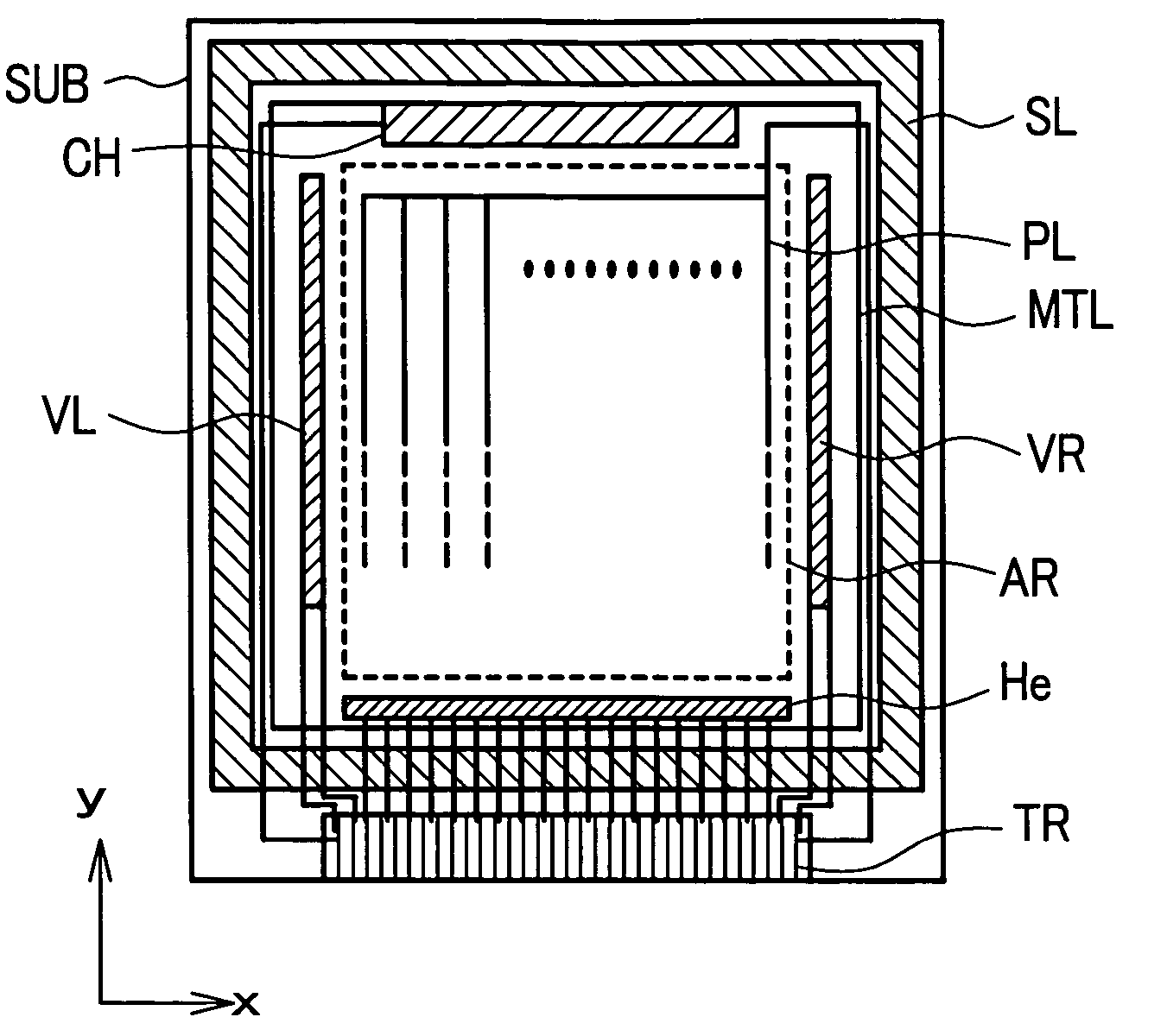
[0043] Embodiments of an organic EL display device according to the present invention are explained hereinafter in conjunction with drawings.

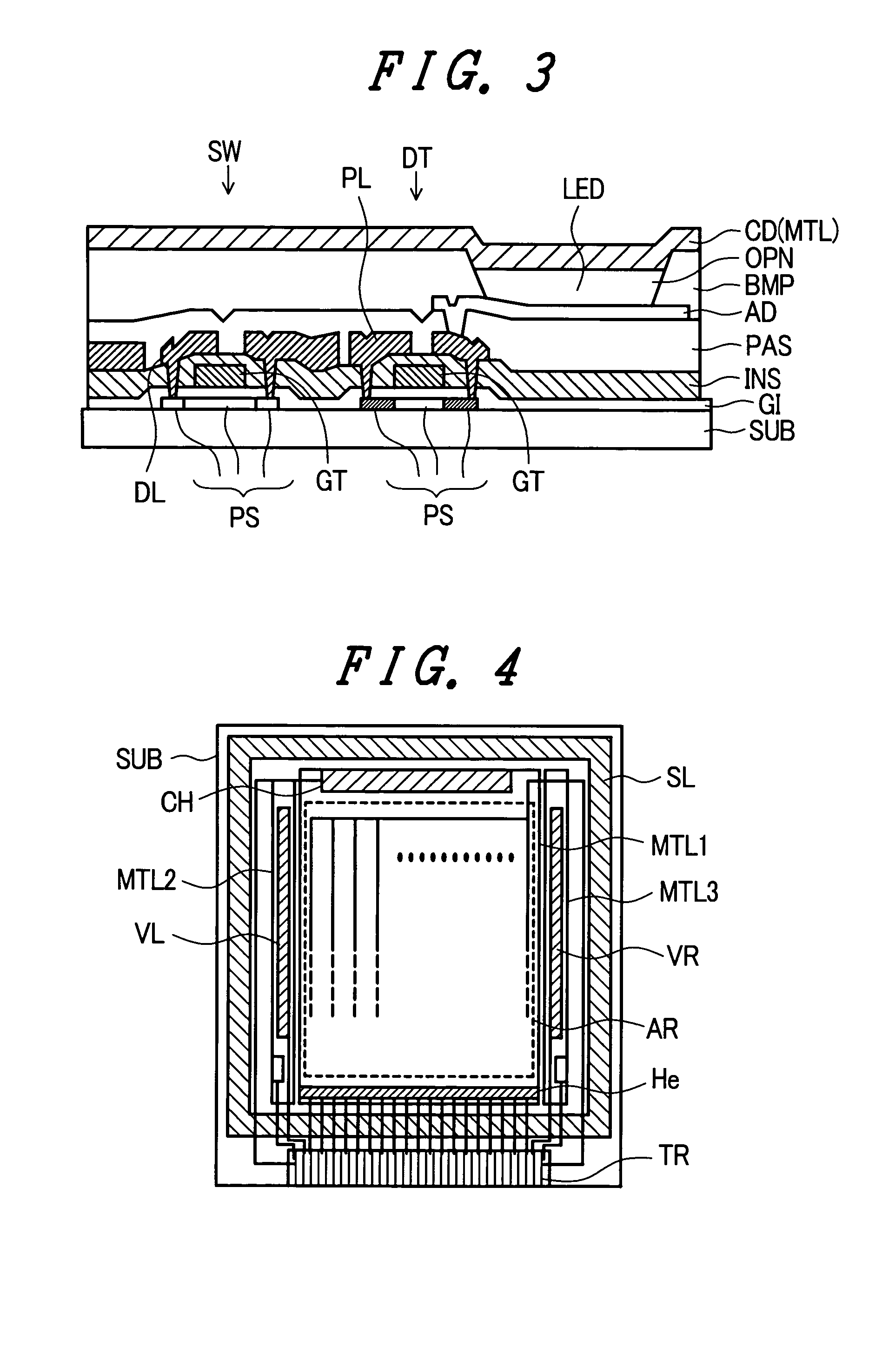
[0044]FIG. 1 is a schematic plan view showing one embodiment of the constitution of the organic EL display device according to the present invention. First of all, there is provided a transparent substrate SUB which is formed of, for example, a rectangular glass plate.

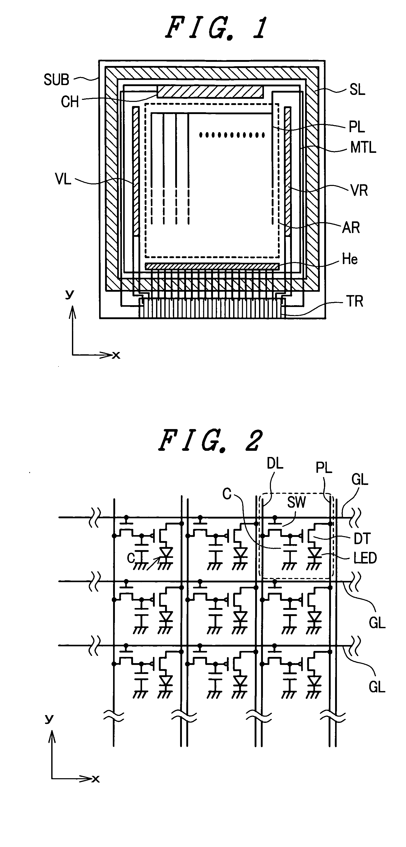
[0045] A display part AR is formed on a center portion of the transparent substrate SUB except for a slight periphery thereof. Although the constitution of the display part AR is described in detail later, a plurality of pixels are arranged in a matrix array, for example, and a plurality of signal lines which run in the x direction as well as in the y direction are formed on boundaries of the respective pixels.

[0046] Then, scanning signal drive circuits VL, VR are formed at both sides, that is, at the left and right sides of the display part AR in a state that the display part ...


PUM


Abstract

The present invention provides an organic EL display device which imparts the flexibility to the pull-around operation of lines. The organic EL display device is characterized in that the display device includes a display part and a display drive circuit which is formed on a periphery of the display part on a surface of a substrate, wherein the display part includes a plurality of pixels driven by the display drive circuit, each one of the pixels is formed of a stacked body which is constituted of at least one electrode, a light emitting layer and another electrode stacked from the substrate side, another electrodes of respective pixels are electrically connected in common, and a conductive layer which is formed on the same layer and is made of the same material as another electrodes is formed on a region other than the display region in a state that the conductive layer is electrically separated from another electrodes.

Description

BACKGROUND OF THE INVENTION [0001] 1. Field of the Invention [0002] The present invention relates to a display device, and more particularly to an organic EL (Electro Luminescence) display device, for example. [0003] 2. Description of the Related Art [0004] An organic EL display device is configured such that a plurality of pixels which are arranged in a matrix array are formed within a display part on a substrate, each one of these pixels is formed of a stacked body which is constituted by stacking at least one electrode, a light emitting layer and another electrode from the substrate side, and an electric current is supplied to the light emitting layer through the electrode thus allowing the light emitting layer to emit light (see Japanese Patent Laid-open Patent Publication 2000-36381, Japanese Patent Laid-open Patent Publication Hei9(1997)-148066). [0005] Further, a so-called active-matrix type display device includes, at least, gate signal lines which are formed along pixel gro...

Claims


Application Information

Patent Timeline
Patent Type & Authority Applications(United States)
IPC IPC(8): G09F9/30H01L51/50H01L27/32H05B33/00H05B33/14
CPCH01L27/3276H01L27/326H10K59/121H10K59/131
Inventor TOKUDA, NAOKISATO, TOSHIHIROAKIMOTO, HAJIMEKAGEYAMA, HIROSHI
Owner SAMSUNG DISPLAY CO LTD
Why Eureka
Try Eureka