Method of manufacturing semiconductor device with electrode for external connection and semiconductor device obtained by means of said method

a manufacturing method and semiconductor technology, applied in semiconductor devices, semiconductor/solid-state device details, electrical devices, etc., can solve the problems of difficult application of such insulation methods to semiconductor packaging processes, difficult application of such insulation methods to semiconductor processes, and desire for wiring without electrodes. , to achieve the effect of easy removal, low cost and imparting flexibility to the connection pattern

Active Publication Date: 2011-09-13
INVENSAS CORP
View PDF8 Cites 42 Cited by
  • Summary
  • Abstract
  • Description
  • Claims
  • Application Information

AI Technical Summary

Benefits of technology

[0029]According to the present invention, the internal connection electrode structure of a double-sided electrode package can be realized simply and at low cost, without requiring a through electrode technique. Thus, the double-sided electrode package can be effectively used in the field of compact mounting of electronic equipment to a cellular phone or the like, and effectively used as a package for a sensor whose three-dimensional connection is effective in the electronic equipment.
[0030]Further, according to the present invention, it becomes possible to extend an arbitrary number of wiring lines to arbitrary locations on the upper and lower portions of a substrate, to enable rewiring to be freely performed on the upper surface of the substrate, to thereby impart flexibility to the pattern of connection with an upper side IC.
[0031]Moreover, the present invention utilizes the characteristics of a pattern plated on an electroforming mother die of stain steel or the like such that the pattern can easily be removed through application of heat and pressure. Thus, the present invention enables the electroforming mother die to be removed without performing an upper surface grading process after resin sealing. Thus, an inexpensive double-sided electrode package can be realized. Further, when a rewiring pattern is formed on a stainless steel plate together with internal connection electrodes, a double-sided electrode package having rewiring on the upper surface thereof can be simply realized without new rewiring.
[0032]Conventionally, formation of internal connection electrodes and wiring are performed in different processes, resulting in an increase in the number of steps, and an increase in cost. For example, conventionally, internal connection electrodes are formed as follows. Holes are formed after resin sealing, and a metal is charged into the holes through plating. In a wiring process, through sputtering or vapor deposition, a metal film is uniformly applied onto metal surfaces exposed to the upper surface, and in a subsequent lithography process, wiring is formed through patterning. Such a method requires complicated processes, and requires processes different from a conventional assembly process, whereby cost tends to increase. In contrast, continuously performing formation of internal connection electrodes and wiring means that these processes are combined into a single process of forming a component including internal connection electrodes and wiring, and in the assembly process, all the conventional processes become unnecessary, whereby cost can be lowered. Further, when a company specialized in manufacture of components manufactures such a component, rationalization through specialization becomes possible, and the processes become simple as a whole, and cost can be lowered.
[0033]Further, according to the present invention, a plurality of elements, such as a sensor element and a processing LSI therefor, can be mounted in a common package, to thereby reduce the size and cost. Thus, it becomes possible to provide a thin image sensor module in which an image sensor and a signal processing IC are integrally mounted, or a camera module to which a lens therefor is attached.

Problems solved by technology

Since existing methods for forming through electrodes involve low-temperature treatment so as to charge a low resistance metal, application of such methods to a semiconductor process is difficult.
Further, since existing insulation methods for through holes in a semiconductor substrate involve high-temperature treatment, application of such insulation methods to a semiconductor packaging process is difficult.
Formation of through electrodes in a semiconductor substrate and insulation for the through electrodes still involve problems to be solved; therefore, wiring that does not require through electrodes is desired.
Such a conventional method has a considerable problem in terms of cost.
Although the upper wiring substrate simultaneously enables extension of electrodes to the upper surface and rewiring, its low cost manufacture is difficult.
This technique requires a considerable complicated process, and increases cost.
Patent Document 5 discloses a technique for integrating a plurality of circuits and elements by use of a double package; however, this document does not disclose a technique for integrating a plurality of circuits and elements within a single common package.
However, since both the faces of the substrate are used, a mounting process becomes complex, which increases cost.
Further, since the opposite faces are covered by components, connection points which are used for attachment to the lens or the main board are present only in a peripheral area of the substrate, so the substrate has a problem of an increased area.[Patent Document 1] Japanese Patent Application Laid-Open (kokai) No. 2001-127243[Patent Document 2] Japanese Patent Application Laid-Open (kokai) No. 2002-158312[Patent Document 3] Japanese Patent Application Laid-Open (kokai) No. 2005-286010[Patent Document 4] Japanese Patent Application Laid-Open (kokai) No. 2003-218283[Patent Document 5] Japanese Patent Application Laid-Open (kokai) No.

Method used


Image

  • Method of manufacturing semiconductor device with electrode for external connection and semiconductor device obtained by means of said method
  • Method of manufacturing semiconductor device with electrode for external connection and semiconductor device obtained by means of said method
  • Method of manufacturing semiconductor device with electrode for external connection and semiconductor device obtained by means of said method

Examples


Embodiment Construction

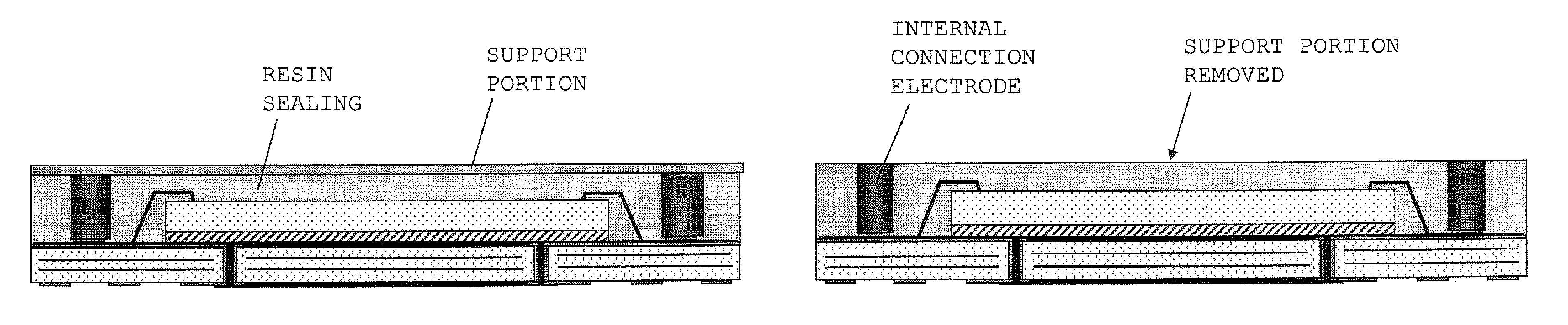
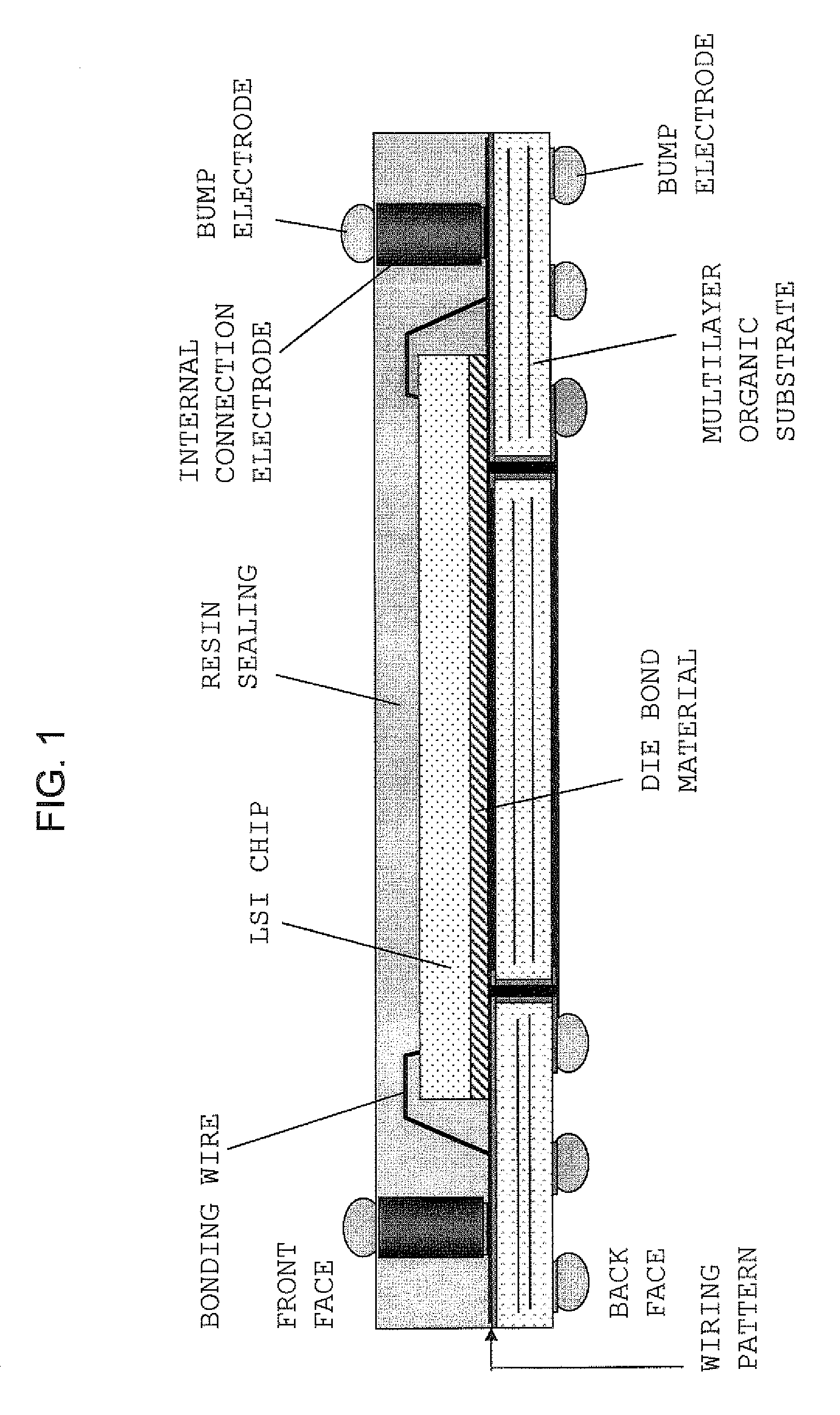
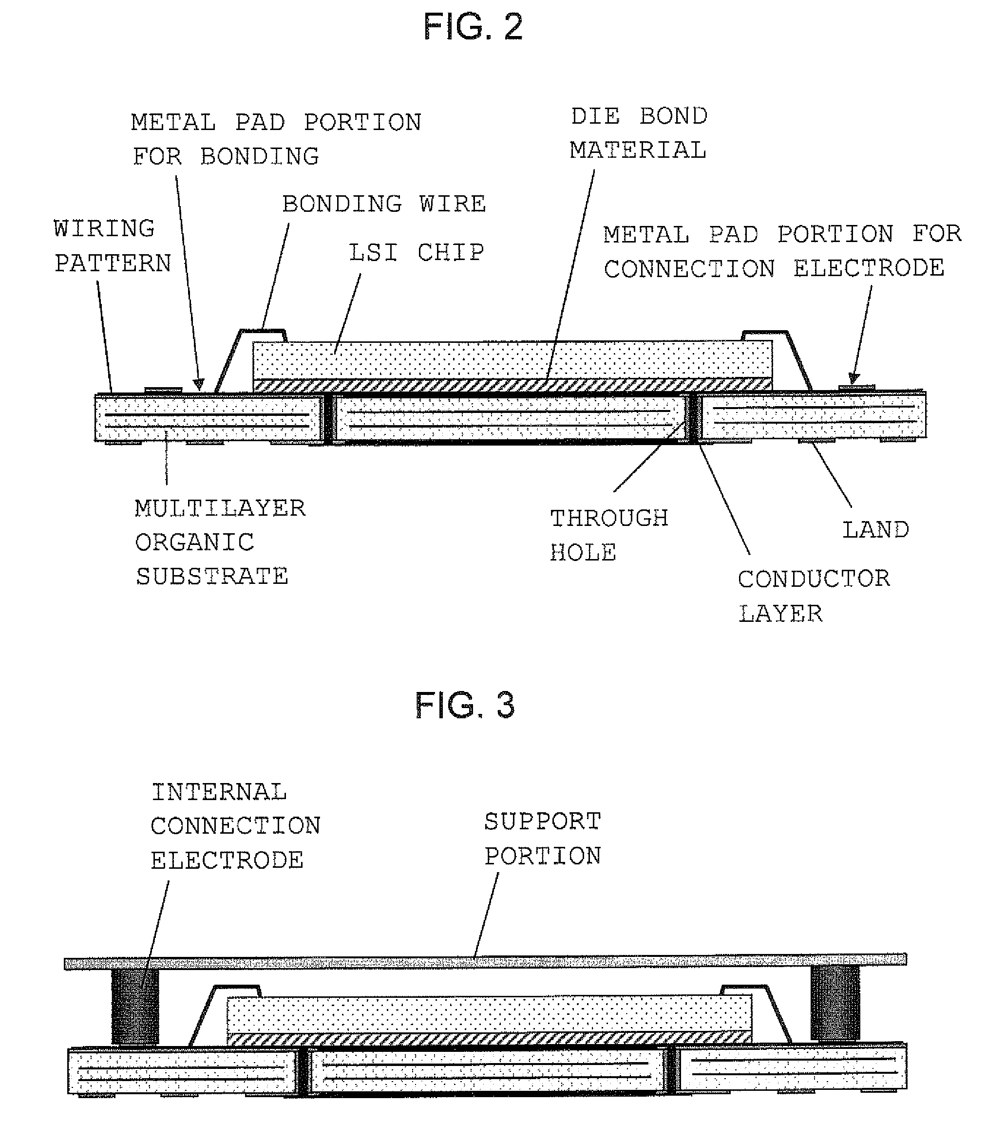
[0083]FIG. 1 shows a cross sectional view of an organic-substrate-type double-sided electrode package showing a first example of a semiconductor device having a double-sided electrode structure of the present invention. As shown in FIG. 1, the organic substrate side of the organic-substrate-type double-sided electrode package will be referred to as the back face, and the side on which a circuit element is disposed on the substrate will be referred to as the front face. A semiconductor chip, such as an LSI chip, is bonded to the multilayer organic substrate by use of a die bond material, and is connected to a wiring pattern of the uppermost layer of the organic substrate by use of bonding wires (wire bond connection scheme). Internal connection electrodes which are formed through electroforming and which are a feature of the present invention are fixed to and electrically connected to the wiring pattern of the organic substrate. The details of manufacture and connection of the intern...


PUM


Abstract

A circuit element is disposed on an organic substrate and is connected to a wiring pattern provided on the organic substrate. Internal connection electrodes are formed on a support of a conductive material through electroforming such that the internal connection electrodes are integrally connected to the support. First ends of the internal connection electrodes integrally connected by the support are connected to the wiring pattern. After the circuit element is resin-sealed, the support is removed so as to separate the internal connection electrodes from one another. Second ends of the internal connection electrodes are used as external connection electrodes on the front face, and external connection electrodes on the back face are connected to the wiring pattern.

Description

CROSS REFERENCE TO RELATED APPLICATIONS[0001]This application is a continuation-in-part application of PCT / JP 2007 / 072157, filed on Nov. 15, 2007.BACKGROUND OF THE INVENTION[0002]1. Field of the Invention[0003]The present invention relates to a method of manufacturing a semiconductor device having a double-sided electrode structure in which circuit elements including a semiconductor chip are disposed and resin-sealed, and electrodes for external connection (hereinafter referred to as “external connection electrodes”) connected to the circuit elements are disposed on both front and back faces; to a method of manufacturing a semiconductor device in which a plurality of circuit elements are disposed, resin-sealed, and are internally connected, and external connection electrodes are to be connected to an outside circuit are disposed; and to semiconductor devices manufactured by these methods.[0004]2. Description of the Related Art[0005]In association with an increase in the degree of in...

Claims


Application Information

Patent Timeline
Patent Type & Authority Patents(United States)
IPC IPC(8): H01L21/00
CPCH01L21/6835H01L23/49517H01L23/49537H01L23/49548H01L23/49816H01L25/105H01L25/03H01L25/0652H01L25/16H01L23/3128H01L2221/68359H01L2224/16H01L2224/48095H01L2224/73265H01L2924/01004H01L2924/01046H01L2924/01078H01L2924/01079H01L2924/12044H01L2924/15311H01L2924/15331H01L2924/19041H01L2924/19105H01L2924/00014H01L24/48H01L2224/32225H01L2224/32245H01L2224/48227H01L2224/48247H01L2924/00H01L2225/06527H01L2225/1035H01L2225/1052H01L2225/107H01L2225/06548H01L2225/06551H01L2225/1011H01L2924/00012H01L2224/451H01L2224/45144H01L24/45H01L2924/181H01L24/73
Inventor ISHIHARA, MASAMICHIUEDA, HIROTAKA
Owner INVENSAS CORP
Why Eureka
Try Eureka