

Semiconductor device having ECC circuit
a technology of ecc circuit and semiconductor device, which is applied in the direction of instruments, coding, code conversion, etc., can solve the problems of soft memory error developing into a major problem, reducing the capacity of the storage node of the cell configuring the memory, and serious problems
- Summary
- Abstract
- Description
- Claims
- Application Information
AI Technical Summary
Benefits of technology
Problems solved by technology
Method used
Image

Examples
first embodiment
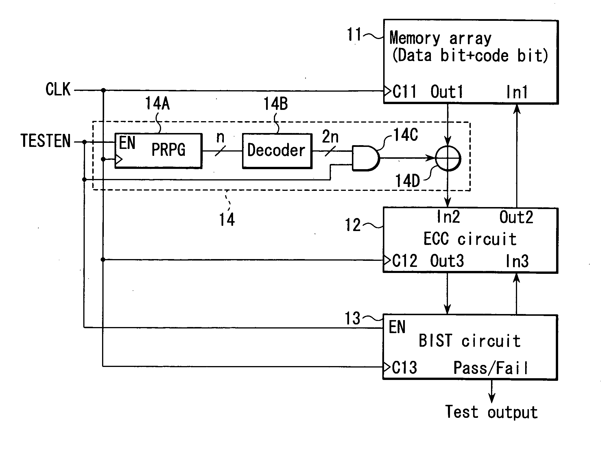
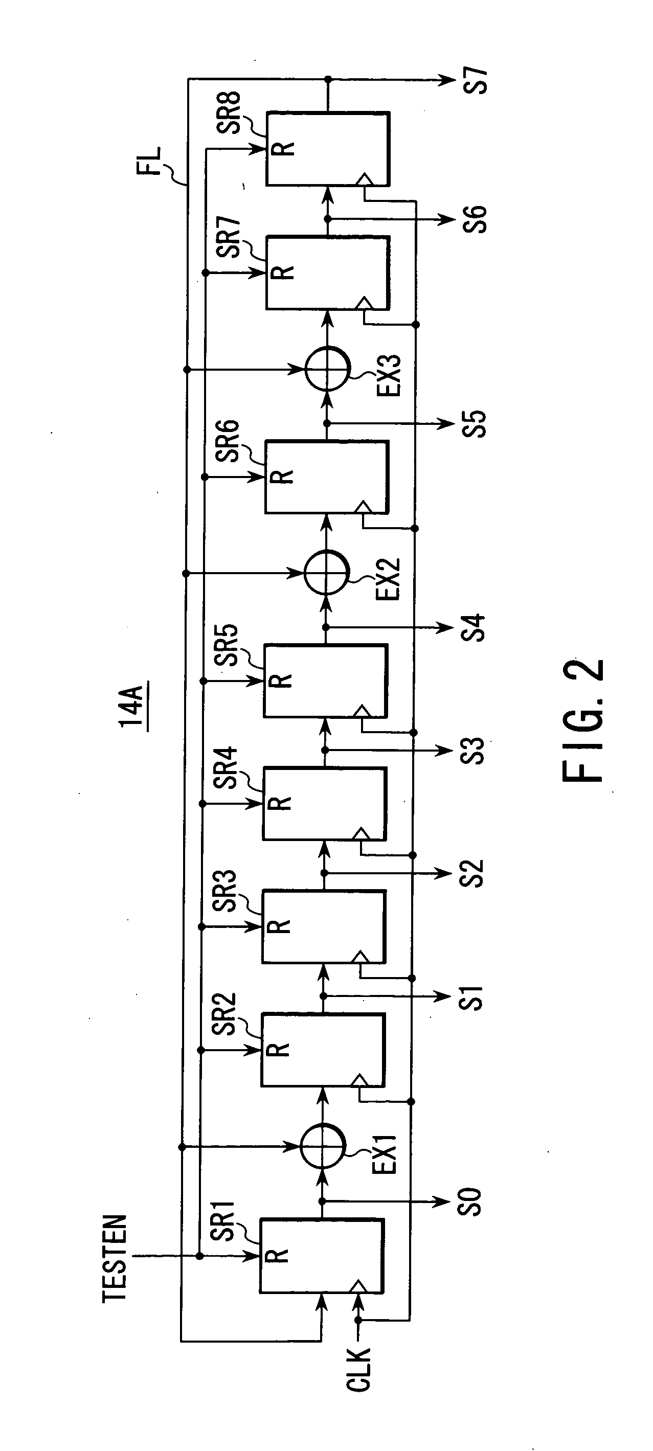
[0023] First, a first embodiment of this invention is explained with reference to FIG. 1. In FIG. 1, a memory array 11 is configured by an SRAM, for example. The memory array 11 stores the total number of bits including a preset number of data bits configuring data and a preset number of error bits of an error correction code as one word unit in each address position. Row and column address decoders which designate address positions of the memory array 11 are attached to the memory array 11, but they are omitted here to make the explanation simple. Further, an input port In1 and output port Out1 which are used to input / output data and a clock input port C11 which receives a clock CLK are provided in the memory array 11.
[0024] The data input port In1 of the memory array 11 is connected to a first output port Out2 of an ECC circuit 12 via a data path and the data output port Out1 is connected to a first input port In2 via another data path. The same clock CLK as that supplied to the ...
second embodiment
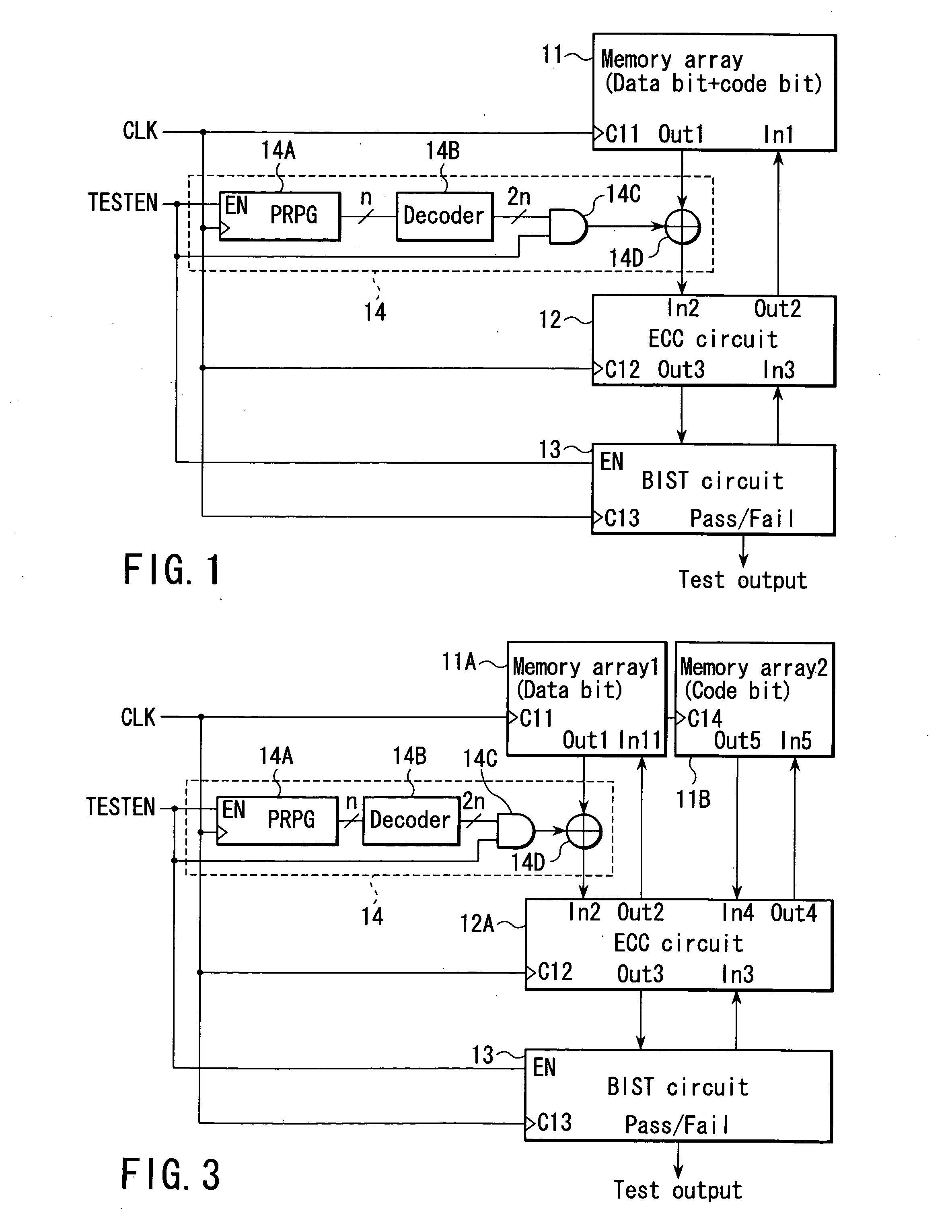
[0035]FIG. 3 is a block diagram showing the configuration of another embodiment of this invention which is configured based on the above idea. In FIG. 3, portions which correspond to those of FIG. 1 are denoted by the same or similar reference symbols and the detail explanation thereof is omitted.
[0036] In the embodiment of FIG. 3, a memory array 11A which stores data bits and a memory array 11B which stores code bits are separately provided. In the memory array 11A, an input port In1 and output port Out1 are provided together with a clock terminal C11. The ports In1 and Out1 are respectively connected to an output port Out2 and input port In2 of an ECC circuit 12A. Like the embodiment of FIG. 1, the ECC circuit 12A includes an input port In4 and output port Out4 together with a clock terminal C12 in addition to an input port In3 and output port Out3 connected to a BIST circuit 13. The input port In4 and output port Out4 are respectively connected to an output port Out5 and input p...
third embodiment
[0041] An embodiment of FIG. 4 is configured based on the above idea and a circuit using a code capable of correcting a 1-bit error and also capable of detecting a 2-bit error is used in an ECC circuit 12B.
[0042] In the embodiment of FIG. 4, portions which correspond to those of FIG. 1 are denoted by the same or similar reference symbols and the repetitive explanation thereof is omitted. In FIG. 4, the ECC circuit 12B has a terminal DED through which a signal indicating detection of a 2-bit error is output when the 2-bit error is detected. For example, an “H” level detection signal appears on the terminal DED when a 2-bit error is detected.
[0043] A BIST circuit 13A includes a BIST circuit section 13A-1 which receives an error correction output from the ECC circuit 12B, an OR circuit 13A-2 which receives a Pass / Fail output of “H” or “L” level of the BIST circuit section 13A-1 at one input terminal, and a latch circuit 13A-3 which latches an output of the OR circuit 13A-2. A detecti...
PUM
 Abstract
Description
Claims
Application Information