
Fully-depleted-collector silicon-on-insulator (SOI) bipolar transistor useful alone or in SOI BiCMOS

a technology of bipolar transistors and collectors, applied in the field of bipolar transistors, can solve the problems of unacceptably large collector series resistance, and achieve the effect of being ready to us

Inactive Publication Date: 2005-04-28
GLOBALFOUNDRIES US INC
View PDF2 Cites 64 Cited by
  • Summary
  • Abstract
  • Description
  • Claims
  • Application Information

AI Technical Summary

Benefits of technology

The present invention describes a new structure for bipolar transistors on SOI that allows for the formation of both npn and pnp transistors on a single chip. The transistors have a unique structure that reduces base-collector junction capacitance and does not require a heavily doped subcollector layer. The transistors use thin-silicon SOI and are compatible with high-speed CMOS devices. The invention also provides an integrated circuit chip that includes both bipolar transistors and MOSFETs. The technical effects of the invention include smaller device size, improved performance, and compatibility with high-speed devices.

Problems solved by technology

The resulting collector series resistance is unacceptably large.

Method used


Image

  • Fully-depleted-collector silicon-on-insulator (SOI) bipolar transistor useful alone or in SOI BiCMOS
  • Fully-depleted-collector silicon-on-insulator (SOI) bipolar transistor useful alone or in SOI BiCMOS
  • Fully-depleted-collector silicon-on-insulator (SOI) bipolar transistor useful alone or in SOI BiCMOS

Examples


Embodiment Construction

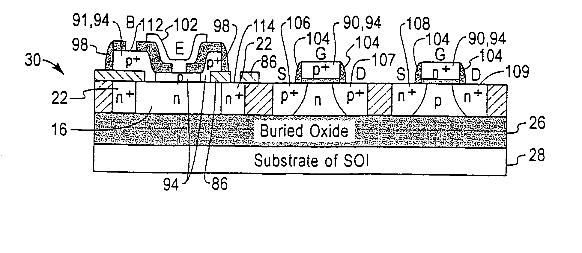
[0031] The basic structure of the fully-depleted-collector SOI npn bipolar transistor 10 is illustrated in FIG. 6. Bipolar transistor 10 has an emitter 12 of n+ type semiconductor, a base 14 of p type semiconductor and a collector 16 having a depleted n collector region 18 and a quasi-neutral n collector region 20. An n+ type semiconductor region 22 contiguous with quasi-neutral n collector region 20 provides a low impedance reachthrough for electrical connection to circuit wiring. As shown in FIG. 6, emitter 12 is over base 14. Base 14 is over collector region 18 and does not contact collector region 20. Collector region 20 is positioned between collector region 18 and n+ type semiconductor region or reachthrough 22. Collector regions 18 and 20 and n+ type semiconductor region 22 are positioned over buried oxide layer 26. Below buried oxide layer 26 is over substrate 28. Silicon-on-Insulator 30 comprises semiconductor regions 14, 18, 20 and 22, buried oxide 26 and substrate 28. Ele...


PUM


Abstract

A bipolar transistor structure is described incorporating an emitter, base, and collector having a fully depleted region on an insulator of a Silicon-On-Insulator (SOI) substrate without the need for a highly doped subcollector to permit the fabrication of vertical bipolar transistors on semiconductor material having a thickness of 300 nm or less and to permit the fabrication of SOI BiCMOS. The invention overcomes the problem of requiring a thick semiconductor layer in SOI to fabricate vertical bipolar transistors with low collector resistance.

Description

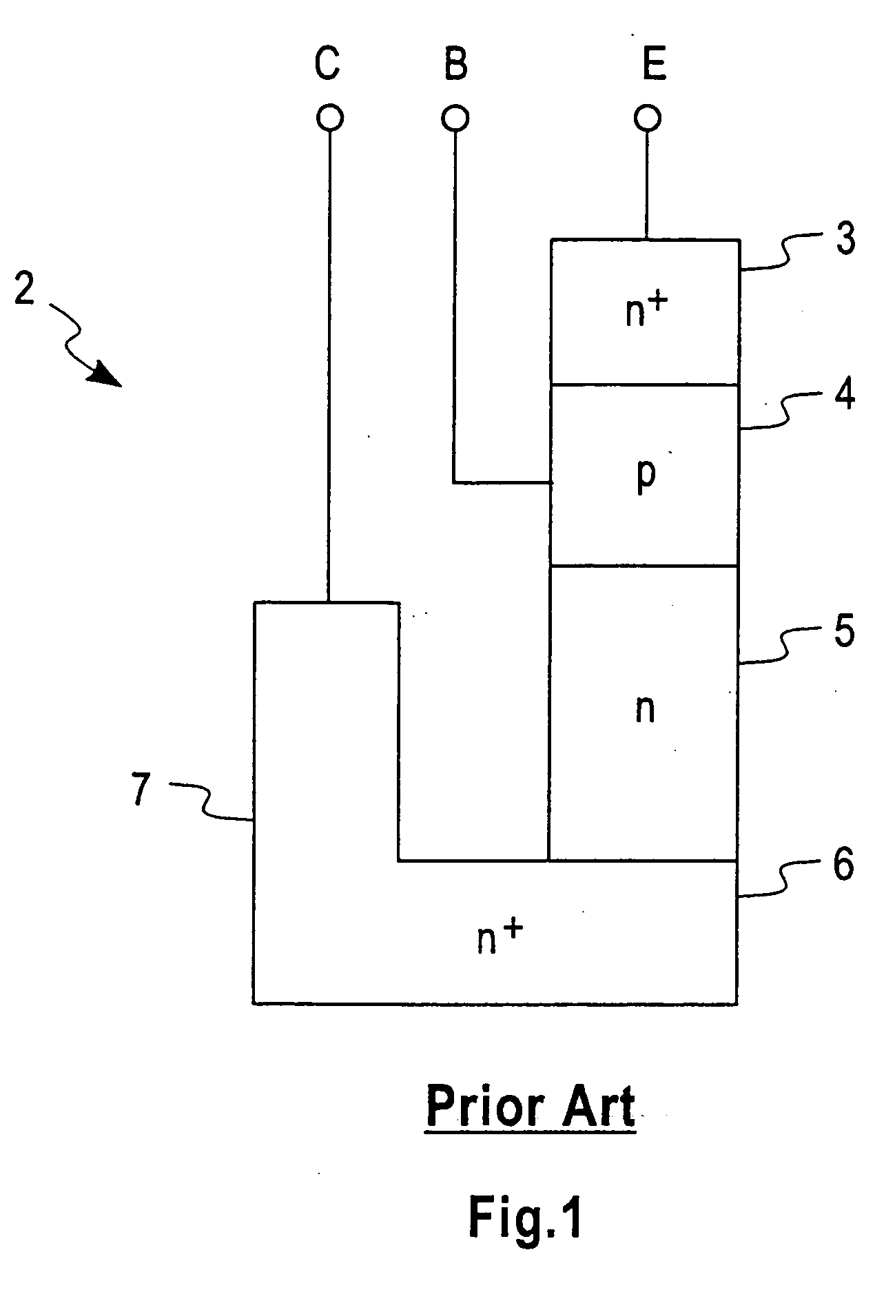
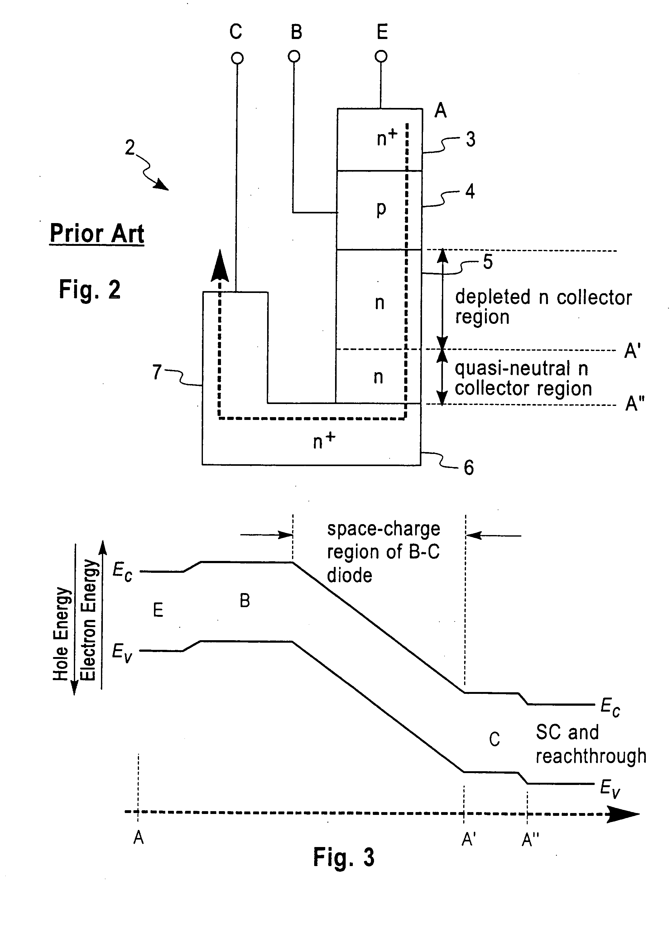
FIELD OF THE INVENTION [0001] This invention relates to bipolar transistors and more particularly to a bipolar transistor structure suitable for implementation on silicon on insulator (SOI) alone or with Complementary Metal Oxide Semiconductor (CMOS) devices to provide SOI BiCMOS essential for most RF and communication products or digital products that have some critical analog components. BACKGROUND OF THE INVENTION [0002] High-performance bipolar transistors are vertical bipolar transistors, as opposed to lateral bipolar transistors. A vertical bipolar transistor, for example an npn bipolar transistor 2 schematically shown in FIG. 1, comprises an n+ type emitter region 3, a p type base region 4, and an n type collector region 5 stacked one on top of the other. In order to reduce collector series resistance, there is usually an n+ type subcollector layer 6 beneath the collector region 5 and an n+ type reachthrough region 7 is used to bring the collector contact to the surface. [000...

Claims


Application Information

Patent Timeline
Patent Type & Authority Applications(United States)
IPC IPC(8): H01L21/331H01L27/12H01L21/8249H01L29/08H01L29/73
CPCH01L27/1203H01L29/7317H01L29/66265H01L29/0821H01L21/8249
Inventor NING, TAK HUNG
Owner GLOBALFOUNDRIES US INC
Learn More