Semiconductor device

a technology of semiconductor devices and shielding films, applied in the direction of semiconductor devices, semiconductor/solid-state device details, electrical apparatus, etc., can solve the problems of cracks at the border, protection films can be damaged, and cracks can not be sure to inhibit crack propagation, etc., to achieve high reliability

Inactive Publication Date: 2005-04-28
RENESAS TECH CORP
View PDF10 Cites 46 Cited by
  • Summary
  • Abstract
  • Description
  • Claims
  • Application Information

AI Technical Summary

Benefits of technology

[0008] Therefore, an object of the present invention is to solve the problem described above, and more particularly, to surely inhibit crack propagation from the peripheral edge to the inside of an interlayer insulating film to provide a semiconductor device with high reliability.

Problems solved by technology

However, the protection film can be damaged in other occasions in addition to dicing with a dicing saw.
For example, when a multi-layer interlayer insulating film is formed on a semiconductor substrate, a crack occurs inside the interlayer insulating film or at the border of the deposited interlayer insulating film because of difference in hygroscopicity, thermal expansion, and the like.
When a semiconductor device is used under the circumstance of high temperature and high humidity, the interlayer insulating film absorbs moisture, which also causes a crack.
The peripheral edge pattern disclosed in Japanese Patent Laying-Open No. 8-172062, however, cannot surely inhibit the propagation of a crack.
As a result, a crack reaches inside the semiconductor device, which adversely affects the reliability of the semiconductor device.
Similarly, the semiconductor chip disclosed in Japanese Patent Laying-Open No. 3-30357 and the semiconductor device disclosed in Japanese Patent Laying-Open No. 11-340167 cannot solve such a problem.

Method used


Image

  • Semiconductor device
  • Semiconductor device
  • Semiconductor device

Examples


first embodiment

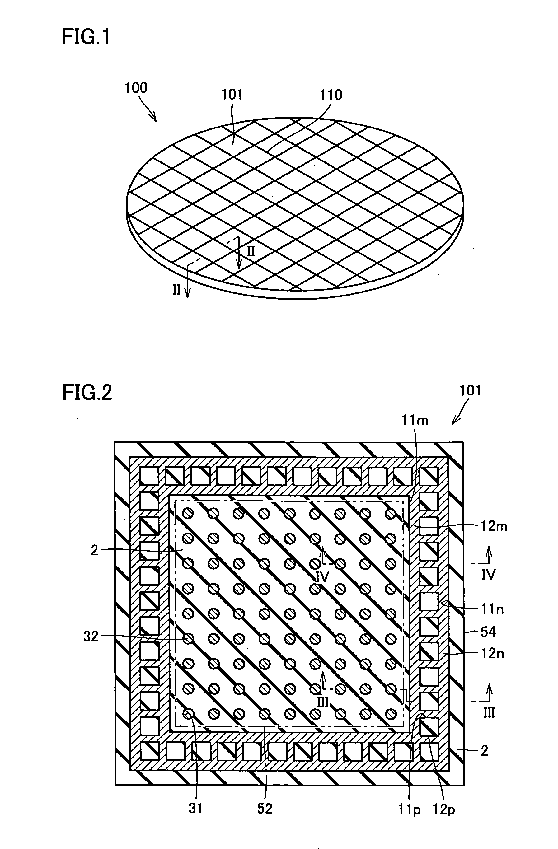
[0025] Referring to FIG. 1, a semiconductor wafer 100 is formed of a silicon substrate and a semiconductor element formed on the silicon substrate. On the surface of the semiconductor wafer, dicing lines 110 are formed in a grid. Semiconductor wafer 100 is diced along dicing lines 110 using a dicing saw to obtain therefrom a semiconductor device 101 in the form of a chip.

[0026] Referring to FIG. 2, a predetermined cross section of semiconductor device 101 obtained from semiconductor wafer 100 in FIG. 1 is shown. Semiconductor device 101 has a rectangular shape in plan view. A peripheral edge 54, which forms the contour of the rectangular shape, is formed of cut surfaces along dicing lines 110. In a memory cell region surrounded by a double-dotted line 52, a memory cell is formed to serve as a semiconductor element.

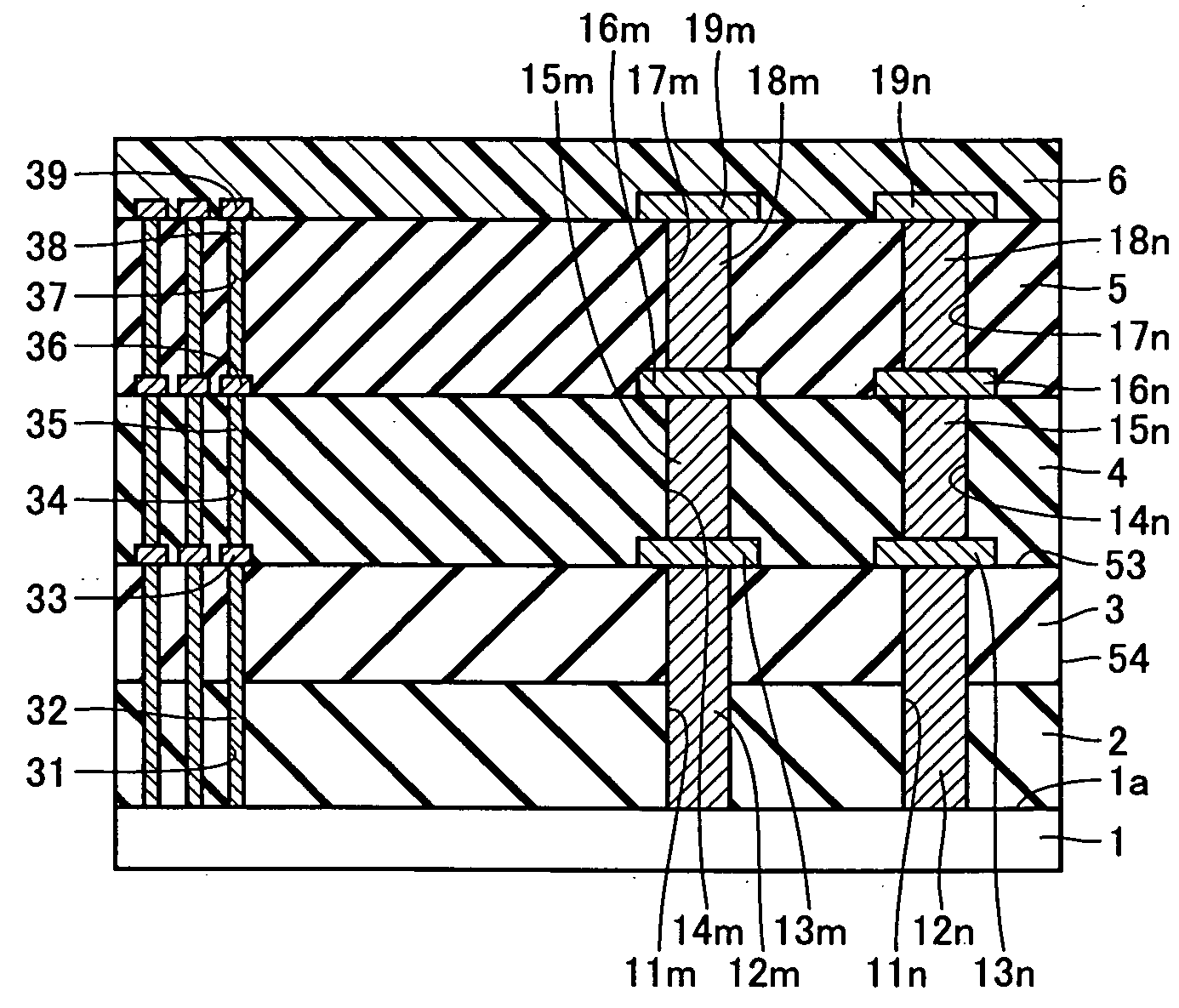
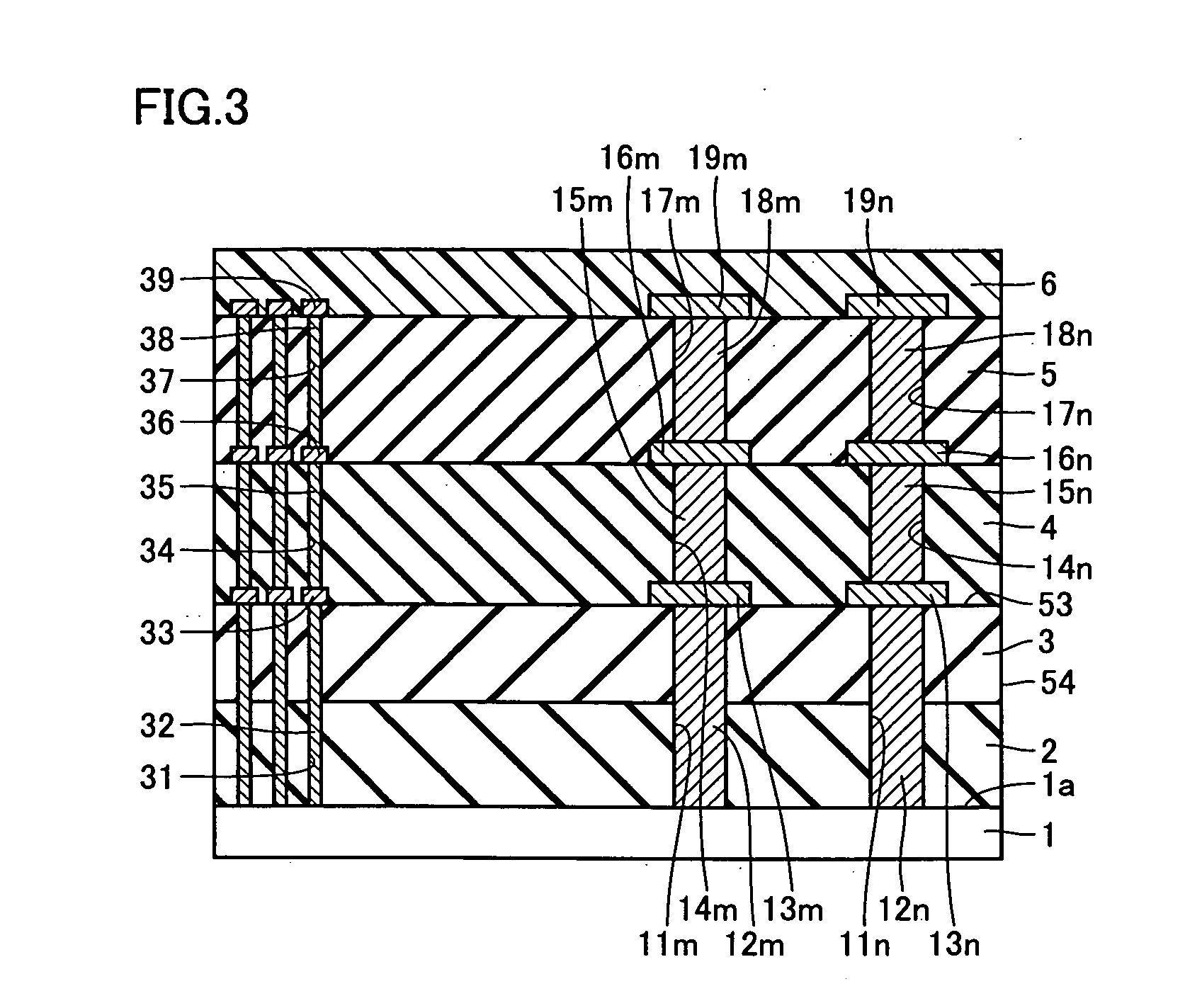
[0027] Referring to FIGS. 2 to 4, interlayer insulating films 2 and 3 are successively formed on a main surface la of a silicon substrate 1. Interlayer insulating film 2...

second embodiment

[0052]FIG. 10 shows a configuration corresponding to a cross section shown in FIG. 2 in the first embodiment. A semiconductor device in a second embodiment has basically the same structure as that of the semiconductor device in the first embodiment, except for the shape of the seal ring formed in the interlayer insulating film. Hereinafter, for the similar structure, description thereof will not be repeated.

[0053] Referring to FIG. 10, in interlayer insulating films 2 and 3, grooves 11m and 11n are formed to be placed outside the memory cell region surrounded by double-dotted line 52, and groove 11p is formed to extend in zigzag between grooves 11m and 11n. Groove 11p connects grooves 11m and 11n at each predetermined spacing. Groove 11p extends in a direction diagonal to the extending direction of grooves 11m and 11n connected by groove 11p.

[0054] According to the semiconductor device configured as such, the effect similar to that of the first embodiment can be obtained. Furtherm...

third embodiment

[0055]FIG. 11 shows a configuration corresponding to a cross section shown in FIG. 2 in the first embodiment. A semiconductor device in a third embodiment has basically the same structure as that of the semiconductor device in the first embodiment, except for the shape of the seal ring formed in the interlayer insulating film. Hereinafter, for the similar structure, description thereof will not be repeated.

[0056] Referring to FIG. 11, in interlayer insulating films 2 and 3, grooves 11m and 11n are formed to be placed outside the memory cell region surrounded by double-dotted line 52, and a plurality of grooves 11p are formed to be placed between grooves 11m and 11n and to extend in a direction orthogonal to the extending direction of grooves 11m and 11n. Grooves 11p protrude from both grooves 11m and 11n, and grooves 11p protruding from one of the grooves extend toward the other groove. Grooves 11p protrude from both grooves 11m and 11n alternately at a predetermined spacing with e...


PUM


Abstract

A semiconductor device includes a silicon substrate having a main surface, a memory cell formed on the main surface, and an interlayer insulating film formed on the main surface to cover the memory cell. The interlayer insulating film has a top surface and a peripheral edge. In the interlayer insulating film, grooves are formed to be placed between the memory cell and the peripheral edge, to extend in parallel with the main surface and to extend in a predetermined direction at a spacing with each other, and a groove is formed to diverge from the grooves and to extend in a direction different from the extending direction of the grooves. The semiconductor device further includes metal film filling the grooves. Thus, crack propagation from the peripheral edge to the inside of the interlayer insulating film can surely be prevented to provide a semiconductor device with high reliability.

Description

BACKGROUND OF THE INVENTION [0001] 1. Field of the Invention [0002] This invention generally relates to a semiconductor device, and more particularly, to a semiconductor device where a multi-layer interlayer insulating film is formed on a semiconductor substrate. [0003] 2. Description of the Background Art [0004] Japanese Patent Laying-Open No. 8-172062 discloses a semiconductor wafer and its manufacturing method which aim at ensuring adhesion between a protection film and functional wiring. The semiconductor wafer disclosed therein has a peripheral edge pattern formed on the protection film along scribe lines along which the wafer is to be diced with a dicing saw, located between the scribe lines and the functional wiring formed in the substrate's region intended for a semiconductor device. The formation of such a peripheral edge pattern can prevent the force, which is applied to a peripheral edge of the protection film along the scribe lines when the wafer is diced with a dicing s...

Claims


Application Information

Patent Timeline
Patent Type & Authority Applications(United States)
IPC IPC(8): H01L23/52H01L21/301H01L21/3205H01L21/4763H01L21/78H01L23/00H01L23/58H01L27/10
CPCH01L23/564H01L23/585H01L2924/0002H01L2924/00H01L21/78
Inventor UESUGI, KATSUHIROMAEDA, KIYOSHITABARU, KENJI
Owner RENESAS TECH CORP
Why Eureka
Try Eureka